Nanometer silicon/monocrystalline silicon heterojunction radial nanowire solar cell and preparation method thereof
A technology of solar cells and silicon nanowires, applied in the field of solar cells, can solve problems such as high surface recombination rate, poor nanowire cells, and low efficiency, and achieve the effects of reducing battery costs, high absorption coefficient, and improving absorption
- Summary
- Abstract
- Description
- Claims
- Application Information
AI Technical Summary
Problems solved by technology
Method used
Image
Examples
example 1
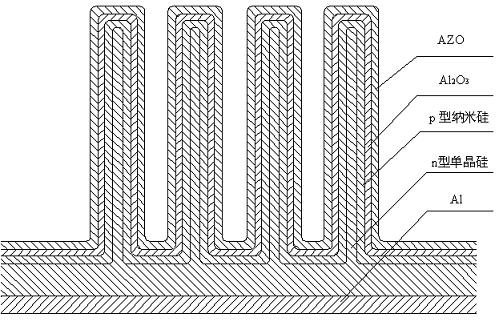
[0041] 1. The structure of monocrystalline silicon / nano-silicon / heterogeneous radial np structure nanowire solar cell see figure 1 ;
[0042] 2. Preparation of solar cells
[0043] 1. Preparation of single crystal silicon nanowires:
[0044] A (100) doped n-type silicon wafer was selected, with a resistivity of 2 Ωcm and a thickness of 200 μm; the n-type (100) silicon wafer was immersed in acetone and ethanol in sequence and ultrasonically cleaned for 10 min to remove organic impurities on the surface, and used to remove Wash with deionized water; then immerse in a mixed solution of sulfuric acid and hydrogen peroxide for 10 min, then wash with deionized water; then immerse the cleaned silicon wafer in HF (4.8 M) and AgNO 3 (10 mM) mixed aqueous solution, stirred slowly, deposited silver particles, and immersed the silicon wafer covered with silver particles in HF (4.8 M) and H 2 o 2 (0.45 M) after corrosion in a mixed aqueous solution for 10 min., the samples were washed...
example 2
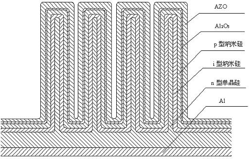
[0057] 1. The structure of nano-silicon / single crystal silicon heterogeneous radial pin structure nanowire solar cell see figure 2 ;
[0058] 2. Preparation of solar cells
[0059] 1. Preparation of single crystal silicon nanowires:
[0060] Select (100) doped n-type silicon wafer with a resistivity of 2 Ωcm and a thickness of 200 μm, and prepare the same as step 1 in Example 1.
[0061] 2. Using PECVD to grow a 20 nm thick intrinsic nano-silicon layer on the silicon nanowire
[0062] Growth conditions: silane with hydrogen dilution ratio of 95%, growth temperature of 250 o C; Silane flow rate 10 sccm,
[0063] The hydrogen flow rate is 40 sccm, and the radio frequency power is 80 W.
[0064] 3. Use PECV to grow a 5nm p-type nano-silicon layer
[0065] Growth conditions: Silane at a hydrogen dilution ratio of 95%, the dilution ratio of borane [PH 3 ] / [PH 3 + H 2 ] is 0.5
[0066] %. Growth temperature 250 o C, silane flow rate 10 sccm, borane flow rate 2 sccm, hyd...
PUM
| Property | Measurement | Unit |
|---|---|---|
| thickness | aaaaa | aaaaa |
| optical band gap | aaaaa | aaaaa |
| thickness | aaaaa | aaaaa |
Abstract
Description
Claims
Application Information


