Interdigital ultraviolet enhanced selective silicon photoelectric diode and manufacture method thereof

An enhanced, interdigitated technology, used in circuits, electrical components, semiconductor devices, etc., can solve the problems of short start, insufficient responsivity and quantum efficiency performance, affecting the performance of ultraviolet detectors, etc. The effect of improving the degree and quantum efficiency, and increasing the area of ​​the depletion layer

Inactive Publication Date: 2011-08-17
XIANGTAN UNIV
View PDF3 Cites 13 Cited by
  • Summary
  • Abstract
  • Description
  • Claims
  • Application Information

AI Technical Summary

Problems solved by technology

However, due to the short start of the p-n junction ultraviolet photodiode, the performance of the proposed stripe photodiode and ultraviolet enhanced photodiode in terms of responsivity and quantum efficiency is not enough, which affects the performance of ultraviolet detectors

Method used


Image

  • Interdigital ultraviolet enhanced selective silicon photoelectric diode and manufacture method thereof
  • Interdigital ultraviolet enhanced selective silicon photoelectric diode and manufacture method thereof
  • Interdigital ultraviolet enhanced selective silicon photoelectric diode and manufacture method thereof

Examples


Embodiment Construction

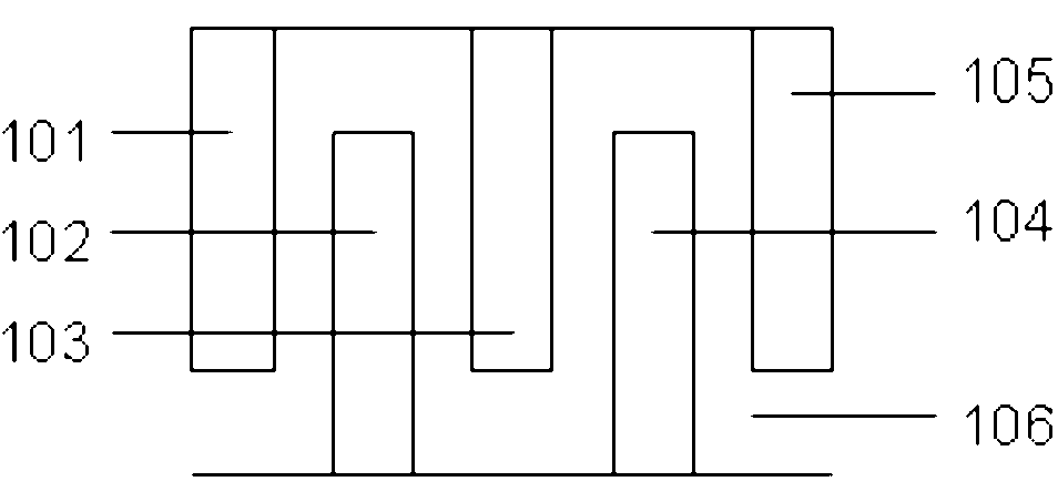
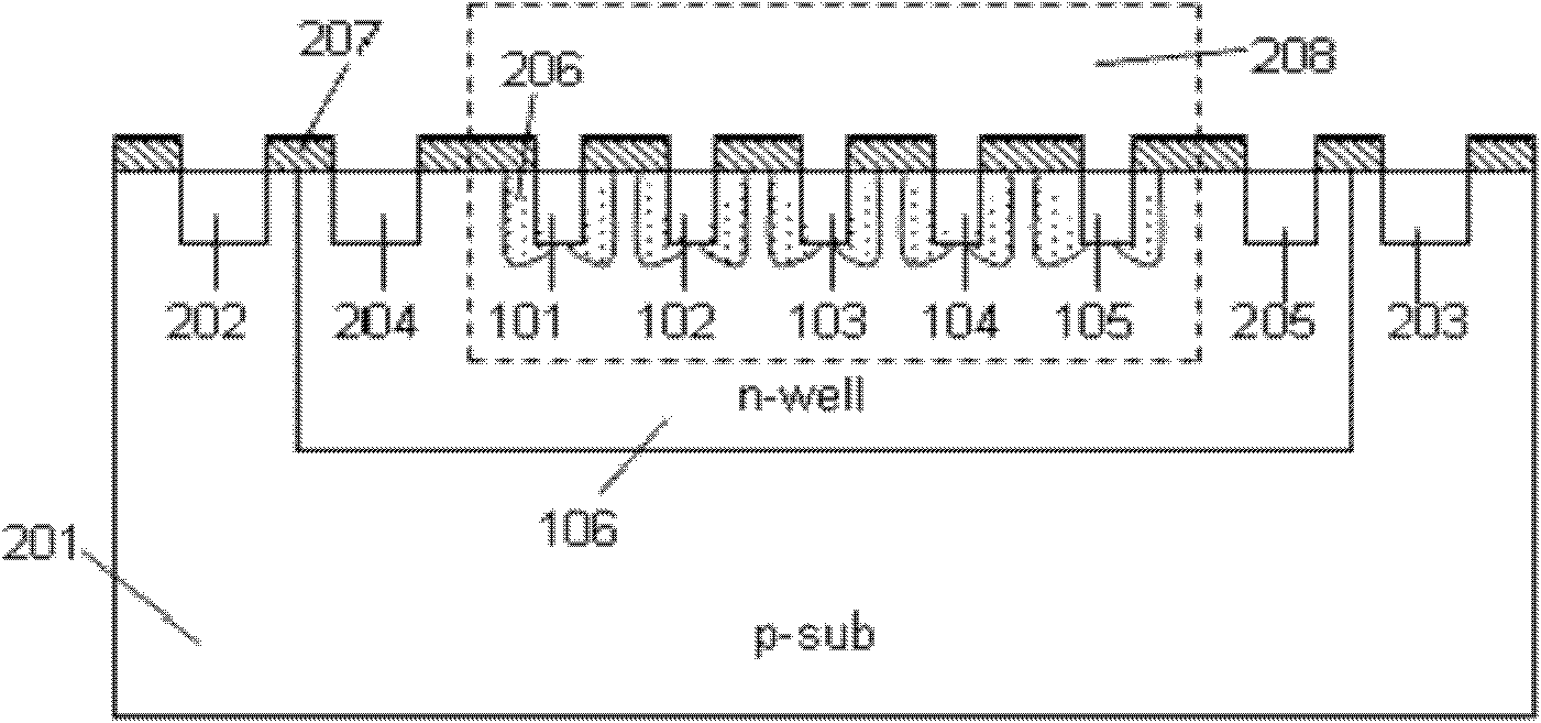
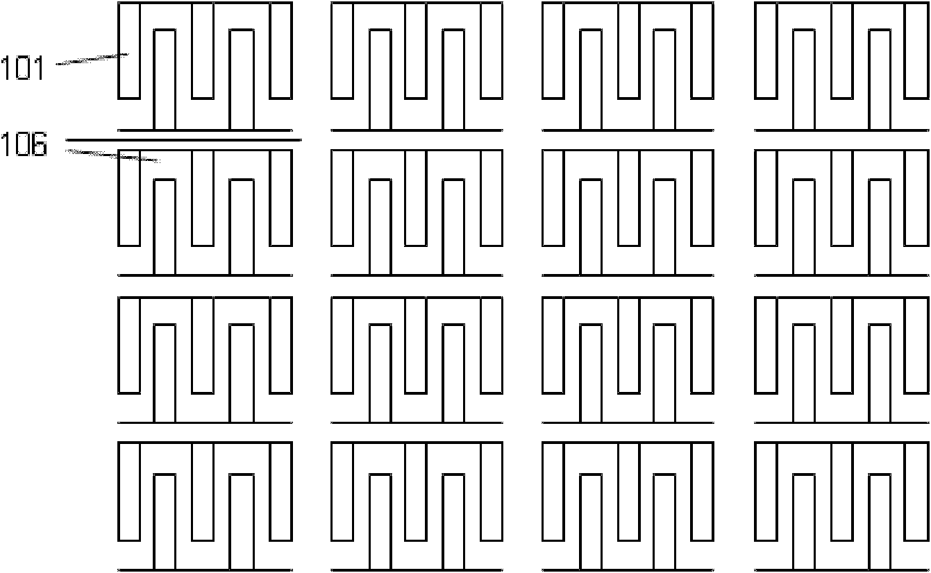
[0029] see figure 1 , figure 1 It is a single interdigitated structure P in the photosensitive area of ​​the present invention + anode structure diagram, figure 1 The photosensitive area in is composed of intersecting P + Doping regions 101, 102, 103, 104, 105 and n-well 106 constitute the interdigitated structure P in this figure + The number of fork indices included in the anode may include more or fewer fork indices.

[0030] see figure 2 , figure 2 In order to realize the ultraviolet enhancement and selection of the internal doping situation and concentration distribution in the photosensitive area of ​​the interdigital structure. It is characterized in that an n-well 106 is implanted in a P substrate 201 and two P + doped regions 202, 203, wherein the n-well 106 and figure 1 Corresponding to the middle n well 106; implant two N in the n well 106 + Doped regions 204 and 205 and five P + Doped regions 101, 102, 103, 104, 105, where P + The doped region 101 cor...


PUM


Abstract

The invention discloses an interdigital ultraviolet enhanced selective silicon photoelectric diode and a manufacture method thereof. The photoelectric diode comprises a P-type substrate, wherein an n well is disposed on the P-type substrate; photosensitive windows on the n well are interdigital or in an array arrangement of interdigital structure; the doping type of the interdigital structure is n-type and p-type alternatively. In the invention, the array arrangement of the interdigital structure is used, the depletion layer area of the diode is increased, and the absorption coefficient of ultrasonic lights is improved, so that the performances of the ultrasonic silicon selective photoelectric diode in the aspects of responsiveness and quantum efficiency are greatly improved; and the diode has wide application prospects in ultrasonic detectors.

Description

technical field [0001] The invention relates to a photodiode, in particular to an interdigitated ultraviolet enhanced selective silicon photodiode and a manufacturing method thereof. Background technique [0002] After more than ten years of research, the performance of ultraviolet photodiodes has been significantly improved in terms of responsivity, quantum efficiency, and integration. The three main ones are photoemission ultraviolet photodiodes, wide bandgap semiconductor ultraviolet photodiodes and p-n junction ultraviolet photodiodes. [0003] Photoemissive UV photodiodes are expensive, bulky and fragile, they are prone to fatigue and aging, making them less sensitive, they must avoid high-intensity radiation, store in a dark place, and require high reverse bias Voltage, these disadvantages limit their application. [0004] Wide bandgap semiconductors, such as SiC, GaN, GaP, AlN, ZnS, and diamond, etc., these materials are difficult to use in the process, the crystal ...

Claims


Application Information

Patent Timeline
Patent Type & Authority Applications(China)
IPC IPC(8): H01L31/107H01L31/0352H01L31/18
Inventor 金湘亮赵永嘉
Owner XIANGTAN UNIV
Why Eureka
Try Eureka