High-speed enhanced ultraviolet silicon selective avalanche photodiode and manufacturing method thereof

An avalanche photoelectric, enhanced technology, applied in circuits, electrical components, semiconductor devices, etc., to achieve the effect of shortening diffusion time, improving selectivity, and improving responsivity

Active Publication Date: 2011-04-20
SHENZHEN AIXIESHENG TECH CO LTD
View PDF5 Cites 19 Cited by
  • Summary
  • Abstract
  • Description
  • Claims
  • Application Information

AI Technical Summary

Problems solved by technology

[0007] In order to solve the technical problems existing in existing photodiodes, the present invention provides a high-speed enhanced ultraviolet silicon selective avalanche photodiode with high sensitivity and fast response speed and its manufacturing method

Method used


Image

  • High-speed enhanced ultraviolet silicon selective avalanche photodiode and manufacturing method thereof
  • High-speed enhanced ultraviolet silicon selective avalanche photodiode and manufacturing method thereof
  • High-speed enhanced ultraviolet silicon selective avalanche photodiode and manufacturing method thereof

Examples


Embodiment Construction

[0029] The following will refer to the attached Figure 2-6 The present invention is described in detail:

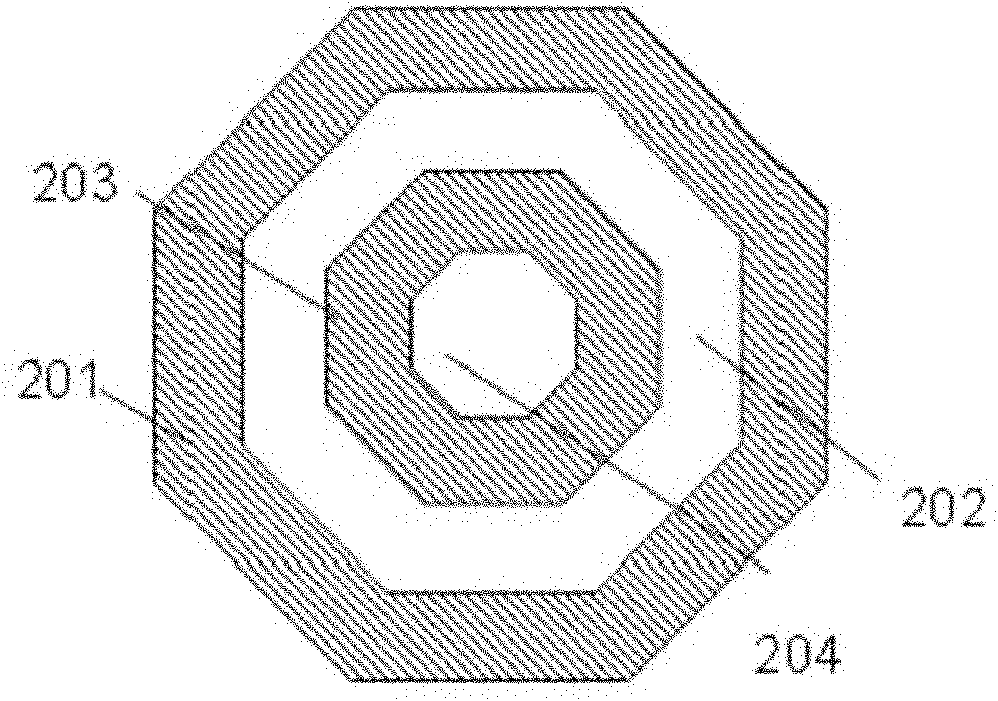
[0030] figure 2 It is the appearance shape of a single regular octagonal photosensitive region, and the pn junction formed between the P+ regions 201, 203 and n-well 202, 204 in the figure is a light absorption region. The number of concentric rings contained in the appearance shape of a single regular octagonal photosensitive area is not the standard as shown in the figure, and may include more regular octagonal concentric rings.

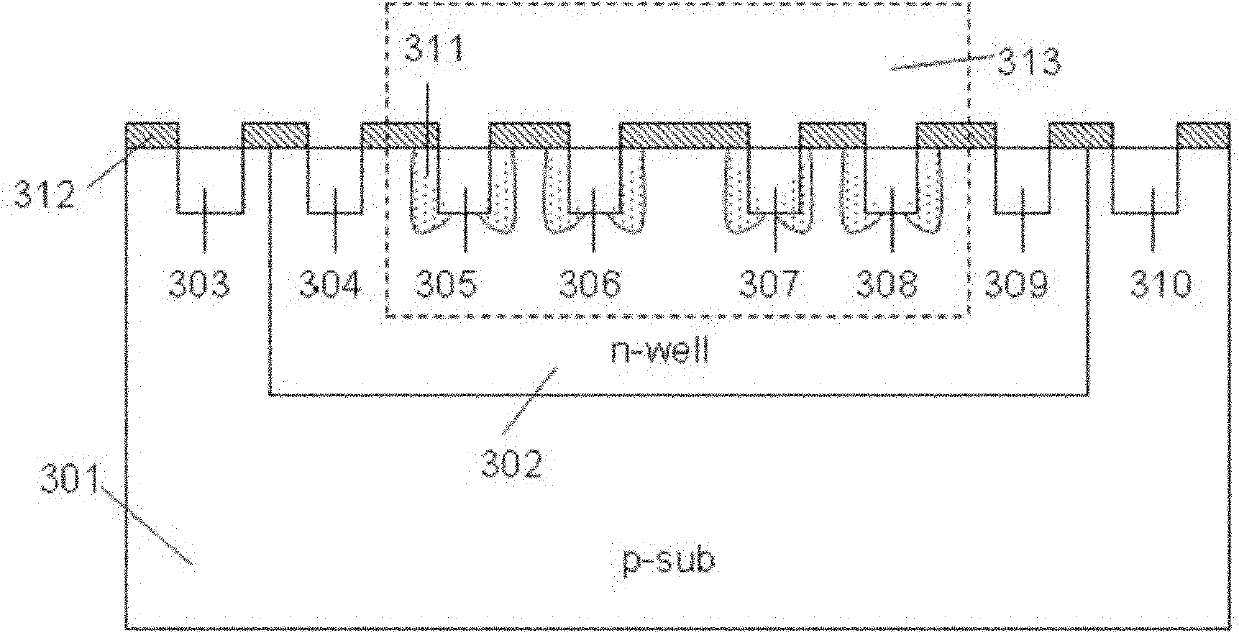
[0031] image 3 It is a structural diagram of the entire interior of a single regular octagonal concentric ring-shaped photosensitive region according to an embodiment of the present invention, and the dotted line box is a regular octagonal concentric ring-shaped photosensitive region. The P+ region in the N well is the anode of the structure, and the N+ region is the cathode of the structure. The P+ region in the P substrate is the read...


PUM


Abstract

The invention discloses a high-speed enhanced ultraviolet silicon selective avalanche photodiode and a manufacturing method thereof. The photodiode comprises a P-type substrate, wherein an n well is arranged on the P-type substrate; a photosensitive window on the n well is a regularly octagonal concentric ring or is in array arrangement of a plurality of regularly octagonal concentric rings; and the doped types of the concentric rings are an n type and a p type at intervals. The photodiode has the advantages of high sensitivity, high responsiveness and high selectivity.

Description

technical field [0001] The invention relates to an avalanche photodiode, in particular to a high-speed enhanced ultraviolet silicon selective avalanche photodiode and a manufacturing method thereof. Background technique [0002] The currently used photodiodes mainly include two types: photoemissive photodiodes, including hollow tube photodiodes, photomultiplier tubes and microchannel photosensitive sheets (MCP); semiconductor photodiodes, which are divided into photocurrent type and photoconductive type. Among them, the photocurrent type is divided into p-n junction type, Schottky barrier type and image sensor, and the p-n junction type is divided into ultraviolet enhanced photodiode, ultraviolet selective photodiode, etc. Photoconductive types include GaAs, GaN, and AlGaN. [0003] Ultraviolet selective gas discharge tubes are widely used in flame detection. It consists of two metal electrodes enclosed in a quartz glass tube filled with hydrogen or a mixture of hydrogen a...

Claims


Application Information

Patent Timeline
Patent Type & Authority Applications(China)
IPC IPC(8): H01L31/107H01L31/0352H01L31/18
Inventor 金湘亮赵永嘉
Owner SHENZHEN AIXIESHENG TECH CO LTD
Why Eureka
Try Eureka