Supercharge Your Innovation With Domain-Expert AI Agents!

Indium phosphide wafer sheet and substrate polishing die for epitaxy wafer sheet

A technology of wafers and indium phosphide, applied in the direction of working carriers, etc., can solve the problems of increasing research and development costs, complex structure of polishing equipment, and reducing processing efficiency, so as to improve production and research and development efficiency, high flatness, and small contact area Effect

Inactive Publication Date: 2019-03-01
SHANGHAI INST OF TECHNICAL PHYSICS - CHINESE ACAD OF SCI
View PDF13 Cites 0 Cited by
  • Summary
  • Abstract
  • Description
  • Claims
  • Application Information

AI Technical Summary

Problems solved by technology

Therefore, due to the special material properties, the current polishing equipment for InP substrate processing has a relatively complicated structure, which increases research and development costs and reduces processing efficiency.

Method used


Image

  • Indium phosphide wafer sheet and substrate polishing die for epitaxy wafer sheet
  • Indium phosphide wafer sheet and substrate polishing die for epitaxy wafer sheet
  • Indium phosphide wafer sheet and substrate polishing die for epitaxy wafer sheet

Examples


Embodiment 1

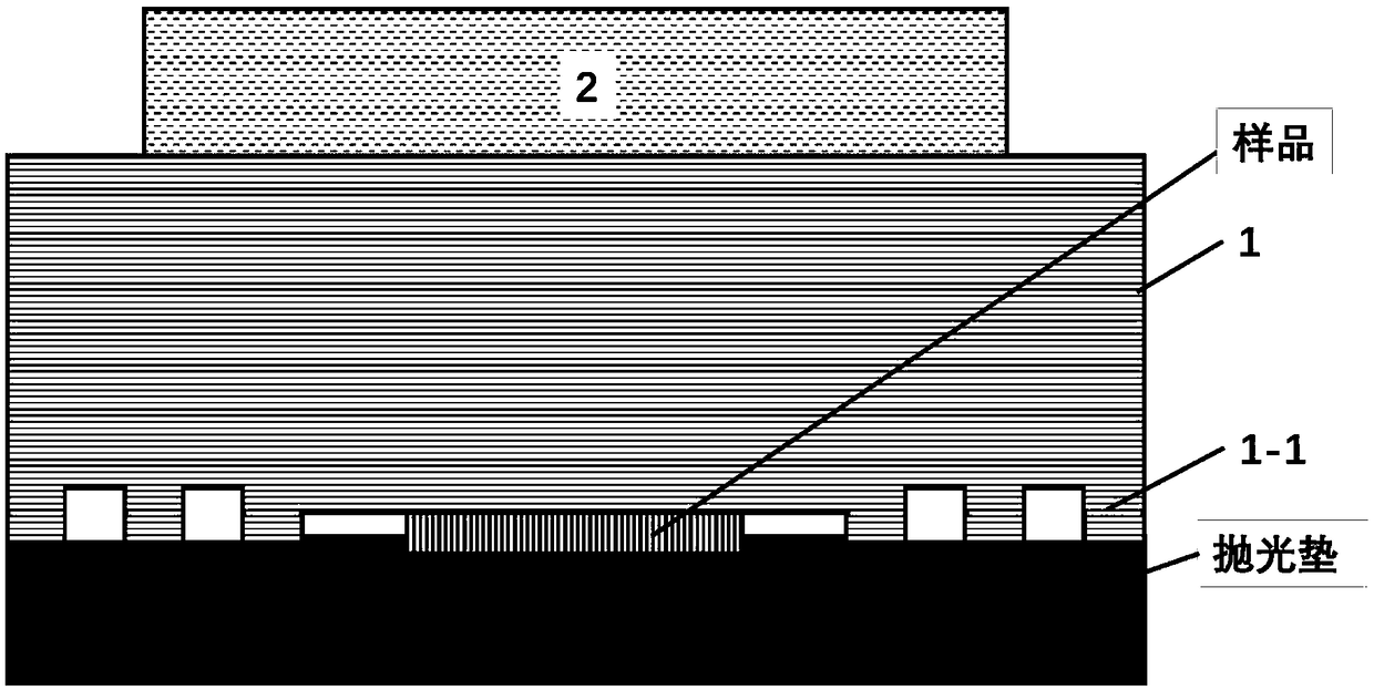
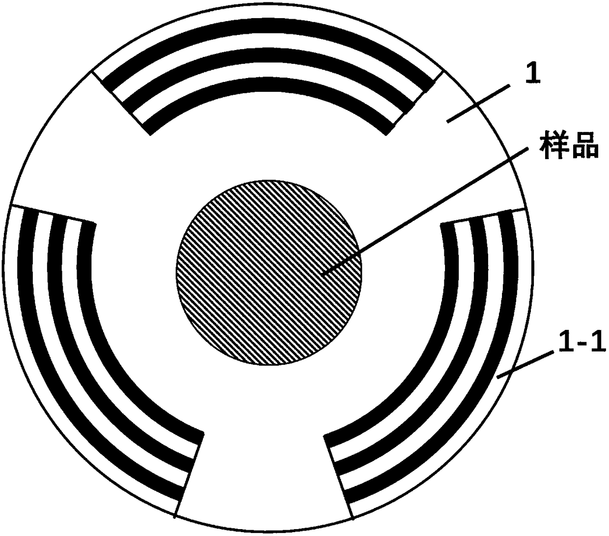
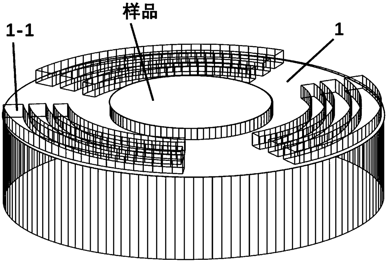
[0024] 1 The height of the ceramic channel is 300 microns, and the groove depth is 0.3 cm.

[0025] 2. Attach a 2-inch InP wafer with a thickness of 350 microns to a ceramic substrate.

[0026] 3. Fix the counterweight so that the sample bears a force of 250g / cm 2 , The speed range of the polishing disc is 80rpm. .

Embodiment 2

[0028] 1 The height of the ceramic channel is 100 microns, and the groove depth is 0.1 cm.

[0029] 2. A 150-micron thick 3-inch epitaxial indium aluminum arsenic indium phosphide wafer is attached to a ceramic substrate.

[0030] 3 Increase the counterweight to make the sample bear a force of 50g / cm 2 , The speed range of the polishing disc is 30rpm. .

Embodiment 3

[0032] 1 The height of the ceramic channel is 1000 microns, and the groove depth is 0.5 cm.

[0033] 2. Attach a 4-inch epitaxial InGaAs indium phosphide wafer with a thickness of 800 microns to a ceramic substrate.

[0034] 3 Increase the counterweight to make the sample bear a force of 500g / cm 2 , The speed range of the polishing disc is 120rpm.


PUM

PropertyMeasurementUnit
surfaceaaaaaaaaaa
depthaaaaaaaaaa

Abstract

The invention discloses an indium phosphide wafer sheet and a substrate polishing die for an epitaxy wafer sheet. The structure of the substrate polishing die comprises a ceramic channel, a ceramic base plate and a balancing weight. The ceramic channel having the supporting function is formed between a polishing pad and the ceramic base plate. The ceramic channel is additionally formed in the ceramic base plate, by the application of the polishing die, the complexity degree of the polishing die can be reduced, the die can rotate stably in the polishing process, meanwhile, the polishing speed can be increased, thus a substrate with the high smoothness is obtained, and the technology cost is reduced.

Description

technical field [0001] The invention relates to the technical field of wafer-level processing of semiconductor wafer materials, in particular to a polishing mold for indium phosphide wafers and epitaxial wafers thereof. Background technique [0002] Indium phosphide (InP), as an important III-V semiconductor material, has a high breakdown electric field and a high average electron drift velocity. At the same time, its electro-optical conversion efficiency and radiation resistance are also strong. It can be used in optical communications, Microwave, millimeter wave devices, photovoltaic cells, infrared detectors, etc. realize important applications. At present, InP-based materials have been applied in many fields, such as laser diodes, light-emitting diodes, and infrared focal plane devices. [0003] During the preparation of InP-based devices and InP epitaxial materials, wafers need to be polished. At present, the mainstream InP polishing method is chemical mechanical poli...

Claims


Application Information

Patent Timeline
Patent Type & Authority Applications(China)
IPC IPC(8): B24B37/30
CPCB24B37/30
Inventor 于一榛孙夺曹高奇邓双燕杨波邵秀梅李雪龚海梅
Owner SHANGHAI INST OF TECHNICAL PHYSICS - CHINESE ACAD OF SCI
Features
  • R&D
  • Intellectual Property
  • Life Sciences
  • Materials
  • Tech Scout
  • Unparalleled Data Quality
  • Higher Quality Content
  • 60% Fewer Hallucinations
Learn More