Automatic classification package method and system of semiconductor device

A packaging method and semiconductor technology, applied in the direction of semiconductor devices, semiconductor/solid-state device manufacturing, electric solid-state devices, etc., can solve problems such as defects, improve product quality and machine efficiency, improve efficiency and quality, and facilitate monitoring and analysis Effect

Active Publication Date: 2019-03-01
SHENZHEN STS MICROELECTRONICS
View PDF13 Cites 6 Cited by
  • Summary
  • Abstract
  • Description
  • Claims
  • Application Information

AI Technical Summary

Problems solved by technology

[0002] At present, in the packaging process, the yield rate of each station cannot be maintained at 100% all the time, and some defective products will be produced. For defective products, the usual method is to use visual inspection at the current station Manually pick them out, or mark the defective products

Method used


Image

  • Automatic classification package method and system of semiconductor device
  • Automatic classification package method and system of semiconductor device
  • Automatic classification package method and system of semiconductor device

Examples


Example

[0252] According to the first embodiment of the automated hierarchical packaging method for semiconductor devices of the present invention, the traceability information of the semiconductor device includes batch, coordinate, and hierarchical information; the automated hierarchical packaging method checks all components at the processing station of the production line. The semiconductor device is packaged; a plurality of the semiconductor devices are arranged in an array on a carrier.

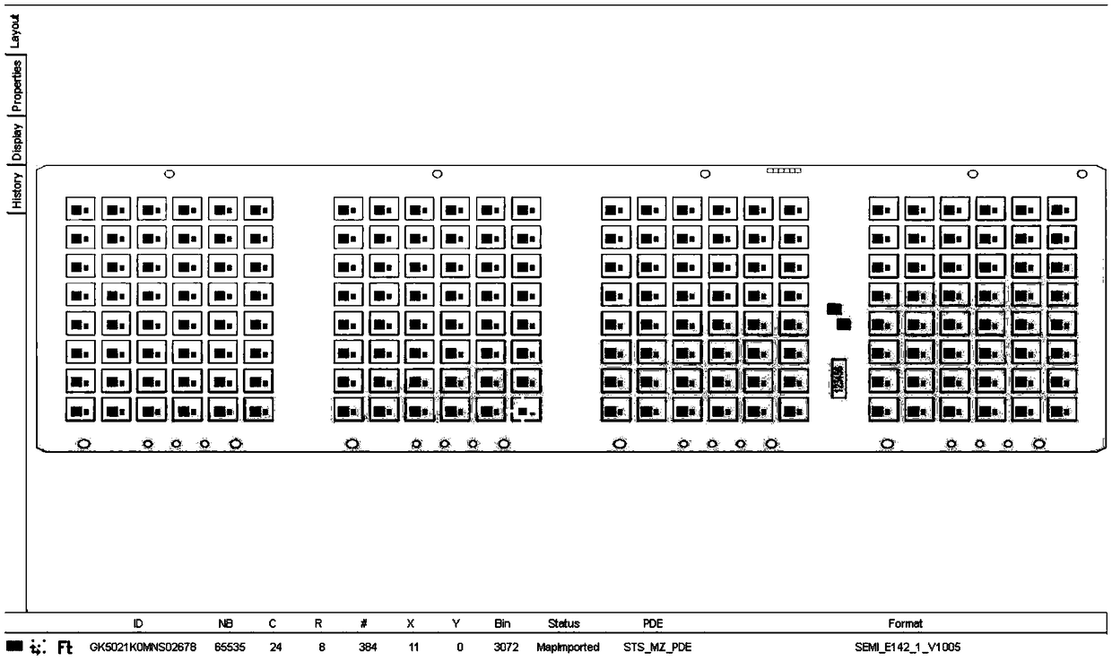
[0253] Understandably, as an example, refer to image 3 And the XML file of the sensor placement station above, in Figure 4 The carrier with STEWOKStrip has four blocks, each block has 8×6 packages, and each package includes two chips: transmitter and sensor. The semiconductor device corresponds to the package, therefore, in Figure 4 In an example, the semiconductor device includes two chips. Therefore, there are three types of traceability information of the semiconductor device: traceability in...


PUM


Abstract

The invention discloses an automatic classification package method of a semiconductor device. Traceability information of the semiconductor device comprises batch, coordinate and classification information. According to the automatic classification package method, the semiconductor device is packaged on a processing station of an assembly line, and a plurality of semiconductor devices are arrangedon a carrier in an array mode. The automatic classification package method at least comprises the following steps of building communication; updating information; downloading updated traceability information of the semiconductor device from a production line management server by a subsequent production line station machine, wherein the semiconductor device with designed classification informationis only processed by the subsequent production line station machine according to the arrangement of the production line management server. By the automatic classification package method, the technical effects of improving product quality and the machine efficiency, saving resources and energy sources and reducing cost are achieved.

Description

technical field [0001] The present invention relates to the technical field (H01L21 / 66) of testing methods or equipment in the process of manufacturing or processing semiconductor devices, and in particular, the present invention relates to an automatic hierarchical packaging method and system for semiconductor devices. Background technique [0002] At present, in the packaging process, the yield rate of each station cannot be maintained at 100% all the time, and some defective products will be produced. For defective products, the usual method is to use visual inspection at the current station Manually pick them out, or mark the defective products with a marker pen, and manually pick out all the defects together after the final station of packaging is completed. There are two obvious disadvantages in this kind of operation: [0003] A) The process of manual operation may come into contact with other good products, but the operator himself is not aware of it, which causes th...

Claims


Application Information

Patent Timeline
IPC IPC(8): H01L21/67H01L21/60
CPCH01L21/67276H01L24/85H01L2224/852
Inventor 曹晶郑旭东
Owner SHENZHEN STS MICROELECTRONICS
Why Eureka
Try Eureka