Micro-LED mass transfer device and transfer method

A transfer device and massive technology, applied in the direction of electrical components, semiconductor/solid-state device manufacturing, circuits, etc., can solve the problems of no electronic components mass transfer method and device, difficult to ensure lateral transfer accuracy, unable to meet large lateral spacing and other problems , to achieve the effect of large application value and simple installation

Active Publication Date: 2019-03-01
GUANGDONG UNIV OF TECH
View PDF6 Cites 39 Cited by
  • Summary
  • Abstract
  • Description
  • Claims
  • Application Information

AI Technical Summary

Problems solved by technology

Due to the expansion of the temporary fixed layer in both the horizontal and vertical directions in this method, it is difficult to ensure the accuracy of the horizontal transfer, and it cannot meet the huge transfer with high horizontal precision requirements, and the expansion of the temporary fixed layer is limited, and it cannot meet the large horizontal spacing.
The mass tr

Method used


Image

  • Micro-LED mass transfer device and transfer method
  • Micro-LED mass transfer device and transfer method
  • Micro-LED mass transfer device and transfer method

Examples


Example Embodiment

[0045] The technical solutions in the embodiments of the present invention will be clearly and completely described below in conjunction with the accompanying drawings in the embodiments of the present invention. Obviously, the described embodiments are only a part of the embodiments of the present invention, rather than all the embodiments. Based on the embodiments of the present invention, all other embodiments obtained by those of ordinary skill in the art without creative work shall fall within the protection scope of the present invention.
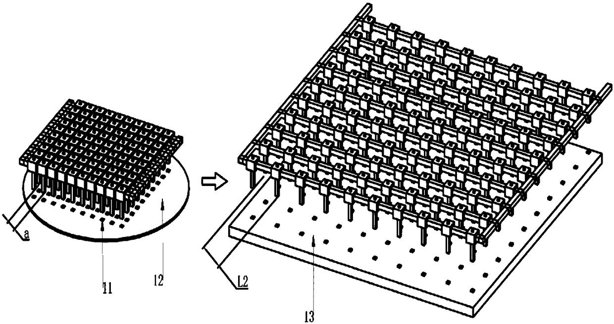
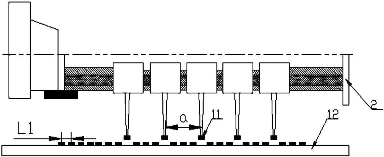
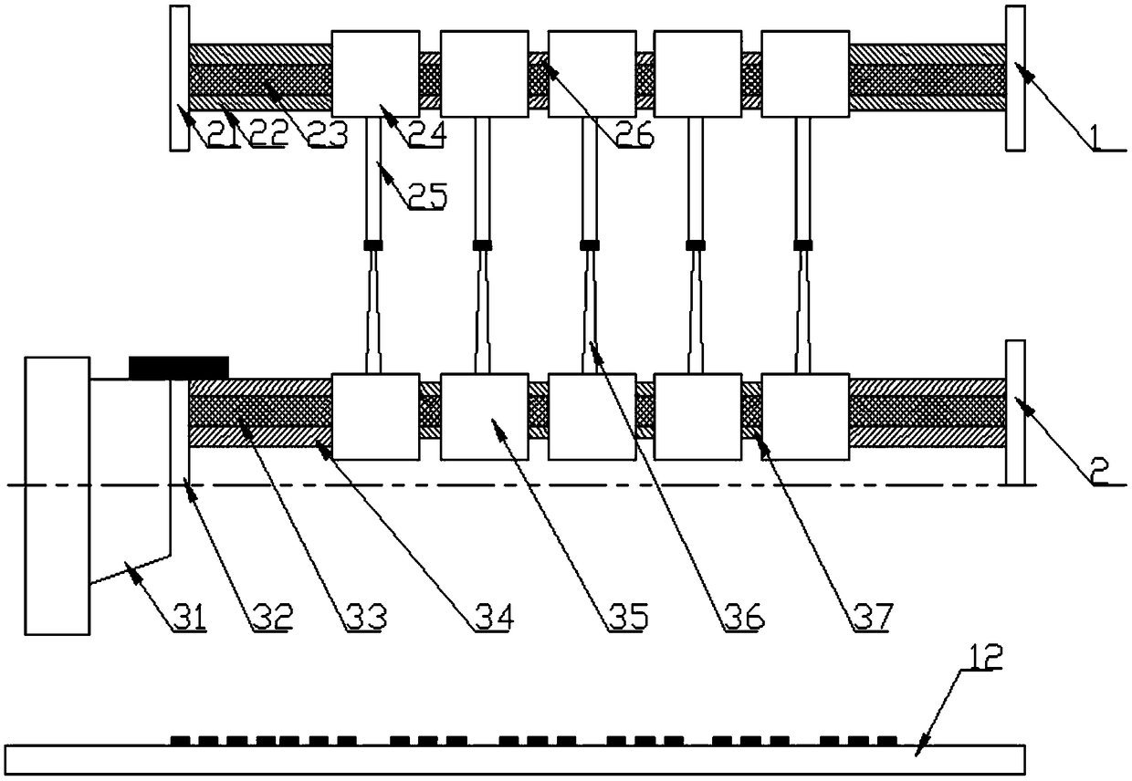
[0046] Such as Figure 1-3 As shown, a micro-LED mass transfer device includes a die-bonding arm 2, a flip-chip soldering arm 3, an external physical field device and a console, a die-bonding arm 2, a flip-chip welding arm 3 and an external physical field The devices are electrically connected to the operating table. The flip chip soldering arm 3 is used to pick up the Micro-LED on the operating table and transfer it to the die-bonding ar...


PUM


Abstract

The invention discloses a Micro-LED mass transfer device. The mass transfer device comprises a die bonding welding arm, a flip chip bonding arm, an external physical field device and an operating table, wherein the die bonding welding arm comprises a die bonding guide rail, a die bonding bracket, a die bonding transfer head and a die bonding elastic telescopic material; and the flip chip welding arm comprises a flip chip rotary motor, a flip chip guide rail, a flip chip bracket, a flip chip transferring head and a flip chip elastic telescopic material. Correspondingly, the invention further provides a Micro-LED mass transfer method. By virtue of the Micro-LED mass transfer device and transfer method provided by the invention, the spacing of the target substrate Micro-LED is only determinedby the transfer head template spacing is overcome in an innovative mode, the rigid structure between the original transfer heads is replaced by the elastic telescopic materials, and the longitudinaldeformation of the elastic telescopic material is changed through the external physical field, so that complete controllable mass transfer of the distance of the electronic elements is realized.

Description

technical field [0001] The present invention relates to the field of semiconductor manufacturing, in particular to a micro-LED mass transfer device and transfer method. Background technique [0002] Micro-LED is a display technology that miniaturizes and matrixes the LED structure, and individually drives and addresses each pixel. Since Micro-LED technology is superior to LCD and OLED technology in various indicators such as brightness, life, contrast, response time, energy consumption, viewing angle and resolution, it is regarded as a new generation of display technology that can surpass OLED and traditional LED. . However, due to the requirements of extremely high efficiency, 99.9999% yield and transfer accuracy within plus or minus 0.5 μm in the packaging process, the size of Micro-LED components is basically less than 50 μm and the number is tens of thousands to millions. -A core technical problem that still needs to be overcome in the process of LED industrialization ...

Claims


Application Information

Patent Timeline
IPC IPC(8): H01L21/67H01L33/48H01L33/62
CPCH01L21/67144H01L33/48H01L33/62H01L2933/0033H01L2933/0066
Inventor 陈新贺云波麦锡全崔成强刘强张凯高健杨志军陈桪陈云汤晖张昱
Owner GUANGDONG UNIV OF TECH
Why Eureka
Try Eureka