
Voltage conversion circuit for photovoltaic module power optimization and capable of generating carrier signal

A voltage conversion circuit and carrier signal technology, applied in photovoltaic power generation, battery circuit devices, circuit devices, etc., can solve problems such as high bit error rate, inaccurate carrier signal, and easy fluctuation of battery output characteristics

Active Publication Date: 2019-03-01
FONRICH NEW ENERGY TECH LTD
View PDF9 Cites 4 Cited by
  • Summary
  • Abstract
  • Description
  • Claims
  • Application Information

AI Technical Summary

Problems solved by technology

Sampling like this to improve the reliability of the signal is only one aspect, but in the case where the photovoltaic cell and the carrier are applied at the same time, the voltage level of the photovoltaic cell itself will be greatly changed due to the influence of the ambient temperature and the intensity of light radiation. , so the distortion of the carrier signal propagating on the power line and the characteristics of the battery, which is easy to fluctuate, are mixed together, resulting in inaccurate real carrier signals that the receiver expects to capture, high bit error rates and photovoltaic cell strings. The superimposed voltage of the group is also subject to carrier interference, so the actual voltage on the entire string may not be within the expected range

Method used


Image

  • Voltage conversion circuit for photovoltaic module power optimization and capable of generating carrier signal
  • Voltage conversion circuit for photovoltaic module power optimization and capable of generating carrier signal
  • Voltage conversion circuit for photovoltaic module power optimization and capable of generating carrier signal

Examples


Embodiment Construction

[0117] Below in conjunction with each embodiment, the scheme of the present invention is clearly and completely set forth, and the described embodiment is only the embodiment that the present invention is used for describing and illustrating but not all embodiments, based on these embodiments, people in the art The solutions obtained by technicians without creative work all belong to the protection scope of the present invention.

[0118] In a switching power supply system, the power supply usually uses a power semiconductor device as a switching element, and the output voltage is adjusted by controlling the duty cycle of the switching element by periodically turning on and off the switch. The switching power supply is mainly composed of input circuit, conversion circuit, output circuit and control unit. Power conversion is its core part, mainly composed of switching circuits, and in some cases, transformers are also applied. In order to meet the requirements of high power de...


PUM


Abstract

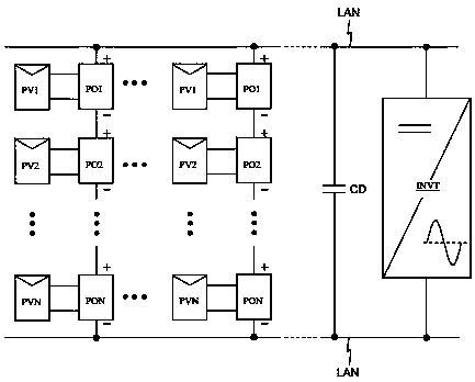
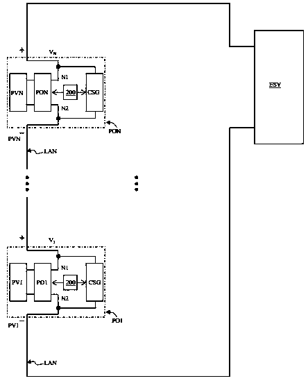
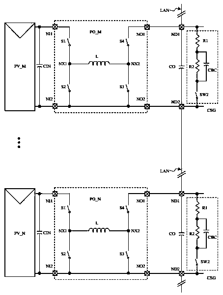
The invention relates to a voltage conversion circuit for photovoltaic module power optimization and capable of generating a carrier signal. The voltage conversion circuit comprises a first inductor,a first switch and a first capacitor, wherein the first inductor is configured on the voltage output path of the voltage conversion circuit used as a switching mode power supply; the first switch andthe first capacitor are connected in series together and are connected in parallel at the two ends of the first inductor. The process of identifying the carrier signal mode in the communication stageof the carrier signal transmitted by the voltage conversion circuit comprises the steps of driving the first switch to be turned off, wherein when a situation that a pulse, taken as a carrier signal,is induced and transiently loaded on a direct current transmission line caused by deficiency of potential difference on the direct current transmission line occurs, it is defined that the carrier signal has a first logic state; and driving the first switch to be connected, wherein when a situation that the pulse, taken as the carrier signal, is induced and transiently loaded on the direct currenttransmission line caused by mixing of potential difference on the direct current transmission line occurs, it is defined that the carrier signal has a second logic state, wherein the logic states characterized by the first logic state and the second logic state of the carrier signal are opposite.

Description

technical field [0001] The present invention mainly relates to the field of photovoltaic power generation. To be precise, it relates to the use of voltage converters that can realize step-down and step-up or buck-boost in applications containing photovoltaic cells, and can determine the pair and voltage according to actual conditions. The target working data of the photovoltaic modules paired with the converter is sent and received by means of carrier communication. Background technique [0002] With the rapid development of the global photovoltaic power generation industry and the high penetration of the Internet, intelligence has become the development trend of photovoltaic power plants. Intelligent power generation, efficient operation and maintenance, and safety management have become industry consensus. Use the professional technology in the field of information and communication to propose intelligent solutions for photovoltaic power plants, build the Internet of Thi...

Claims


Application Information

Patent Timeline
Patent Type & Authority Applications(China)
IPC IPC(8): H02J3/38H02J7/35H04B3/54
CPCH02J3/385H02J7/345H02J7/35H04B3/54Y02E10/56
Inventor 张永
Owner FONRICH NEW ENERGY TECH LTD
Learn More