Semiconductor device and semiconductor integrated circuit

A technology of integrated circuits and semiconductors, applied in the manufacture of semiconductor devices, circuits, and semiconductor/solid-state devices, etc., can solve problems such as power consumption and increase in area, and achieve the effect of reducing heat generation

Active Publication Date: 2019-03-01
SOCIONEXT INC
View PDF20 Cites 1 Cited by
  • Summary
  • Abstract
  • Description
  • Claims
  • Application Information

AI Technical Summary

Problems solved by technology

So in order to get the same as having for example Figure 8 The same saturation current Ion of the FinFET with multi-finger structure shown requires an increase in the number of transistors, resulting in an increase in power consumption and area

Method used


Image

  • Semiconductor device and semiconductor integrated circuit
  • Semiconductor device and semiconductor integrated circuit
  • Semiconductor device and semiconductor integrated circuit

Examples


Embodiment Construction

[0029] Embodiments of the present invention will be described below based on the drawings.

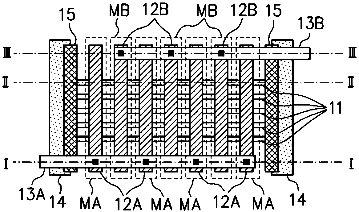
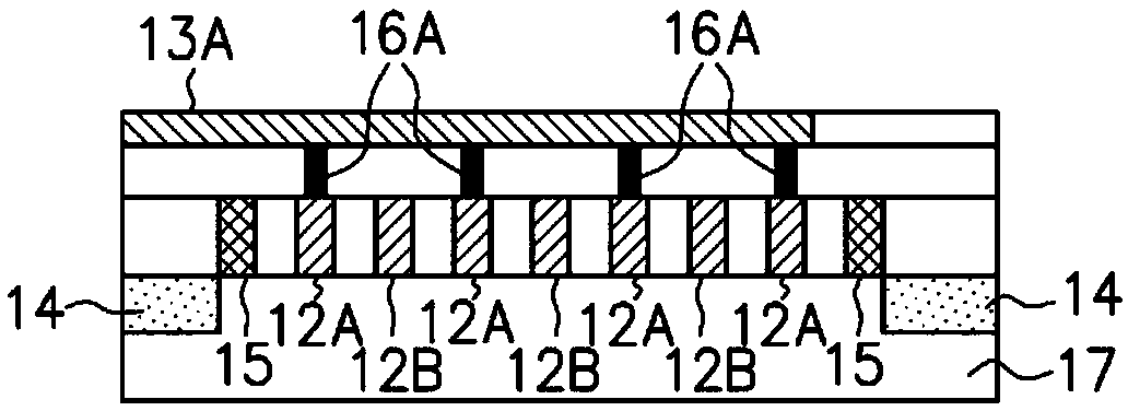
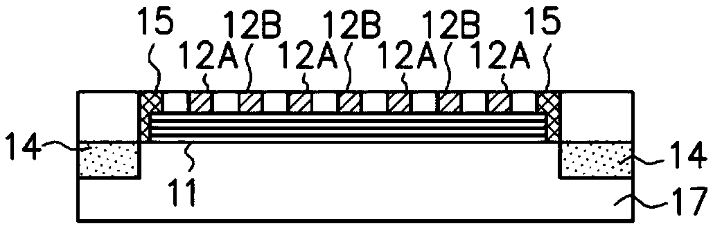
[0030] figure 1 It is a diagram showing a configuration example of a field effect transistor (Fin Field Effect Transistor: FinFET) having a rib-shaped structure as a semiconductor device according to an embodiment of the present invention. Figure 2A is along figure 1 A brief cross-sectional view of the I-I line, Figure 2B is along figure 1 A brief cross-sectional view of the II-II line, Figure 2C is along figure 1 A brief cross-sectional view of line III-III.

[0031] In the FinFET of this embodiment, a convex (fin-shaped) semiconductor region 11 extending in one direction is formed on a substrate 17 . A gate insulating film (not shown) is formed on both side surfaces and an upper surface of a part of the convex semiconductor region 11 . In a part of the convex semiconductor region 11 , gate electrodes 12A and 12B covered with a gate insulating film are formed on both sid...


PUM


Abstract

The present invention provides a semiconductor device and a semiconductor integrated circuit, comprising: element isolation regions (14); projected semiconductor regions (11); a plurality of first gate electrodes (12A) which are formed between a pair of opposing ends of the element isolation regions and each of which is formed on both side surfaces and the top surface of a part of the projected semiconductor region; at least one second gate electrode (12B) which is formed between a pair of the plurality of first gate electrodes in the same layer as the plurality of first gate electrodes, and to which voltage to turn a transistor to an off state is applied; and source regions and drain regions formed in the projected semiconductor regions on both sides of the first gate electrode and the second gate electrode. By disposing, between transistors having the first gate electrodes, a transistor having the second gate electrode to which voltage to turn the transistor to an off state is applied, heat generated in the transistors is reduced without reducing the saturation current of the transistors.

Description

technical field [0001] The present invention relates to a semiconductor device and a semiconductor integrated circuit. Background technique [0002] There is a field effect transistor (Fin Field Effect Transistor: FinFET), which has gates formed on both sides and the upper surface of a part of a convex (fin-shaped) semiconductor region extending in one direction on a substrate. An electrode insulating film and a gate electrode are formed, and a rib-shaped structure of a source region and a drain region is formed in the convex semiconductor regions on both sides of the gate electrode (for example, refer to Patent Document 1). In its structure, FinFET is easy to leave heat, so it is necessary to find a way to reduce heat generation through layout. [0003] Figure 8 It is a diagram showing a configuration example of a FinFET having a multi-finger structure in which a plurality of gate electrodes are formed in a comb-tooth shape (finger shape). exist Figure 8 Among them, 101...

Claims


Application Information

Patent Timeline
Patent Type & Authority Applications(China)
IPC IPC(8): H01L21/336H01L29/78
CPCH01L29/78H01L21/823437H01L29/41758H01L29/4238H01L27/0924H01L29/785H01L29/0642H01L29/0847H01L29/42356H01L29/7851
Inventor 吉谷正章
Owner SOCIONEXT INC
Why Eureka
Try Eureka