Method of forming a fin field effect transistor

A fin field effect and transistor technology, which is applied in semiconductor devices, semiconductor/solid state device manufacturing, electrical components, etc., can solve the problems of poor performance of N-type fin field effect transistors, etc.

Active Publication Date: 2019-08-27
SEMICON MFG INT (SHANGHAI) CORP
View PDF3 Cites 0 Cited by
  • Summary
  • Abstract
  • Description
  • Claims
  • Application Information

AI Technical Summary

Problems solved by technology

[0006] The problem solved by the present invention is that the performance of the N-type fin field effect transistor formed by the method of the prior art is not good

Method used


Image

  • Method of forming a fin field effect transistor
  • Method of forming a fin field effect transistor
  • Method of forming a fin field effect transistor

Examples


Embodiment 2

[0120] The difference between the second embodiment and the first embodiment is as follows:

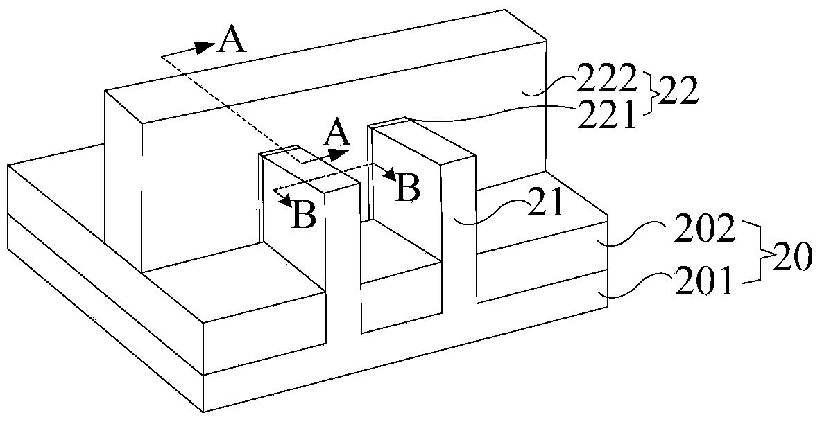
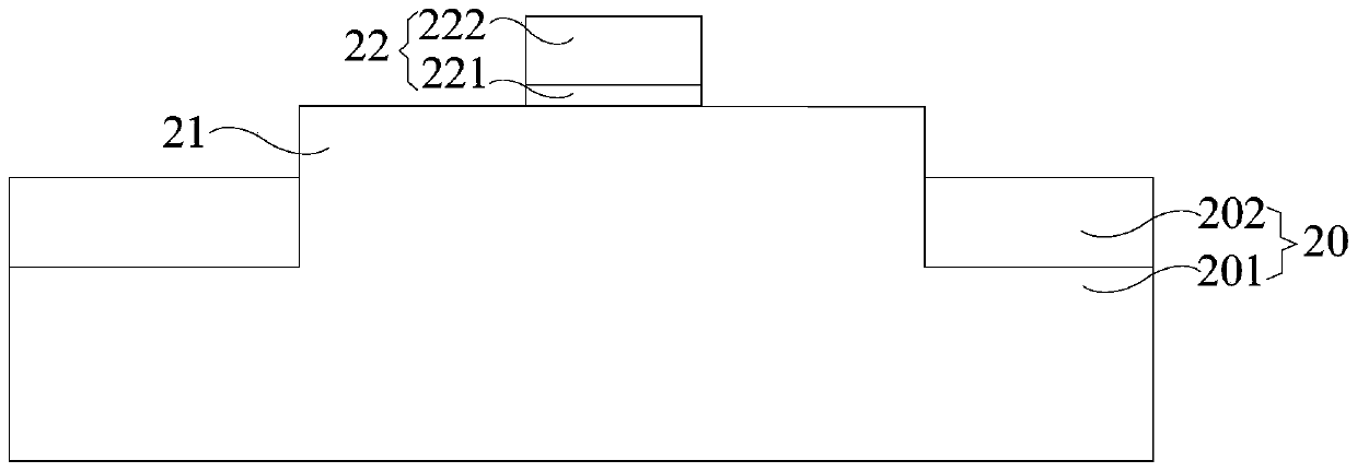
[0121] This embodiment further includes a second region adjacent to the first region, the first region is used to form an N-type fin field effect transistor, and the second region is used to form a P-type field effect transistor. The second region has a second fin. For the method of forming the second fin, please refer to the method of forming the first fin.

[0122] In this embodiment, the second fin is formed simultaneously with the first fin.

[0123] A second polysilicon gate structure is formed across the second fin, the second polysilicon gate structure covers the top and sidewalls of the second fin. The second polysilicon gate structure includes a second gate oxide layer and a second polysilicon layer on the second gate oxide layer.

[0124] In this embodiment, the second polysilicon gate structure is formed simultaneously with the first polysilicon gate structure.

[0125]...


PUM


Abstract

A forming method of a fin type field effect transistor comprises the steps of supplying a substrate which comprises a first area with first fin parts; forming a first gate structure which bestrides the first fin parts; forming a first source electrode material layer and a first drain electrode material layer on the first fins at two sides of the first gate structure; forming a first dielectric layer on the substrate, the first gate structure, the first source electrode material layer and the first drain electrode material layer; forming a first source electrode through hole and a first drain electrode through hole in the first dielectric layer; forming a first metal layer on the source electrode material layer and the first drain electrode material layer; performing first annealing processing on the first metal layer for forming a first high-impedance-phase metal silicide layer; performing ion implantation on the first high-impedance-phase metal silicide layer; and performing second annealing processing on the first high-impedance-phase metal silicide layer after ion implantation, thereby forming a first source electrode metal silicide layer and a first drain electrode metal silicide layer. The forming method can improve performance of a subsequently formed transistor.

Description

technical field [0001] The present invention relates to semiconductor manufacturing, and in particular to a method for forming a Fin Field Effect Transistor. Background technique [0002] With the development of the semiconductor industry to lower technology nodes, the transition from planar CMOS transistors to three-dimensional Fin Field Effect Transistors (FinFETs) has gradually begun. In FinFET, the gate structure can control the channel from at least two sides, which has a much stronger control ability of the gate structure to the channel than planar MOSFET devices, and can well suppress the short channel effect. And compared with other devices, it has better compatibility with the existing integrated circuit production technology. [0003] The formation method of the N-type fin field effect transistor in the prior art is as follows: [0004] First, a semiconductor substrate is provided, the semiconductor substrate having fins. Next, a gate structure across the fin is...

Claims


Application Information

Patent Timeline
Patent Type & Authority Patents(China)
IPC IPC(8): H01L21/336H01L21/28H01L29/78H01L29/45
Inventor 李勇
Owner SEMICON MFG INT (SHANGHAI) CORP
Why Eureka
Try Eureka