Electrostatic discharge circuit and device

An electrostatic discharge circuit and electrostatic discharge technology, applied in circuits, electrical components, electric solid devices, etc., can solve the problems of high instantaneous voltage, chips are easily damaged, and circuit components are burned.

Pending Publication Date: 2019-03-08
合肥博雅半导体有限公司
View PDF0 Cites 1 Cited by
  • Summary
  • Abstract
  • Description
  • Claims
  • Application Information

AI Technical Summary

Problems solved by technology

[0002] Static electricity exists on all kinds of circuit boards, and its instantaneous voltage is very high. Once it cannot be released to the outside, it is likely to burn the circuit components; at present, in the traditional static discharge circuit, when the chip When the negative charge discharge occurs between the power supply terminal, there is usually no direct discharge path, making the chip easy to be damaged

Method used


Image

  • Electrostatic discharge circuit and device
  • Electrostatic discharge circuit and device

Examples


Embodiment Construction

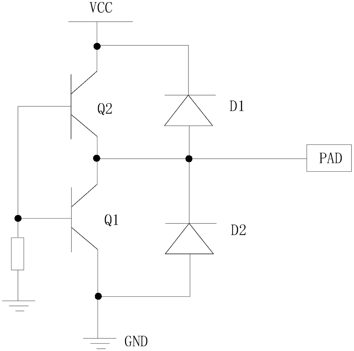
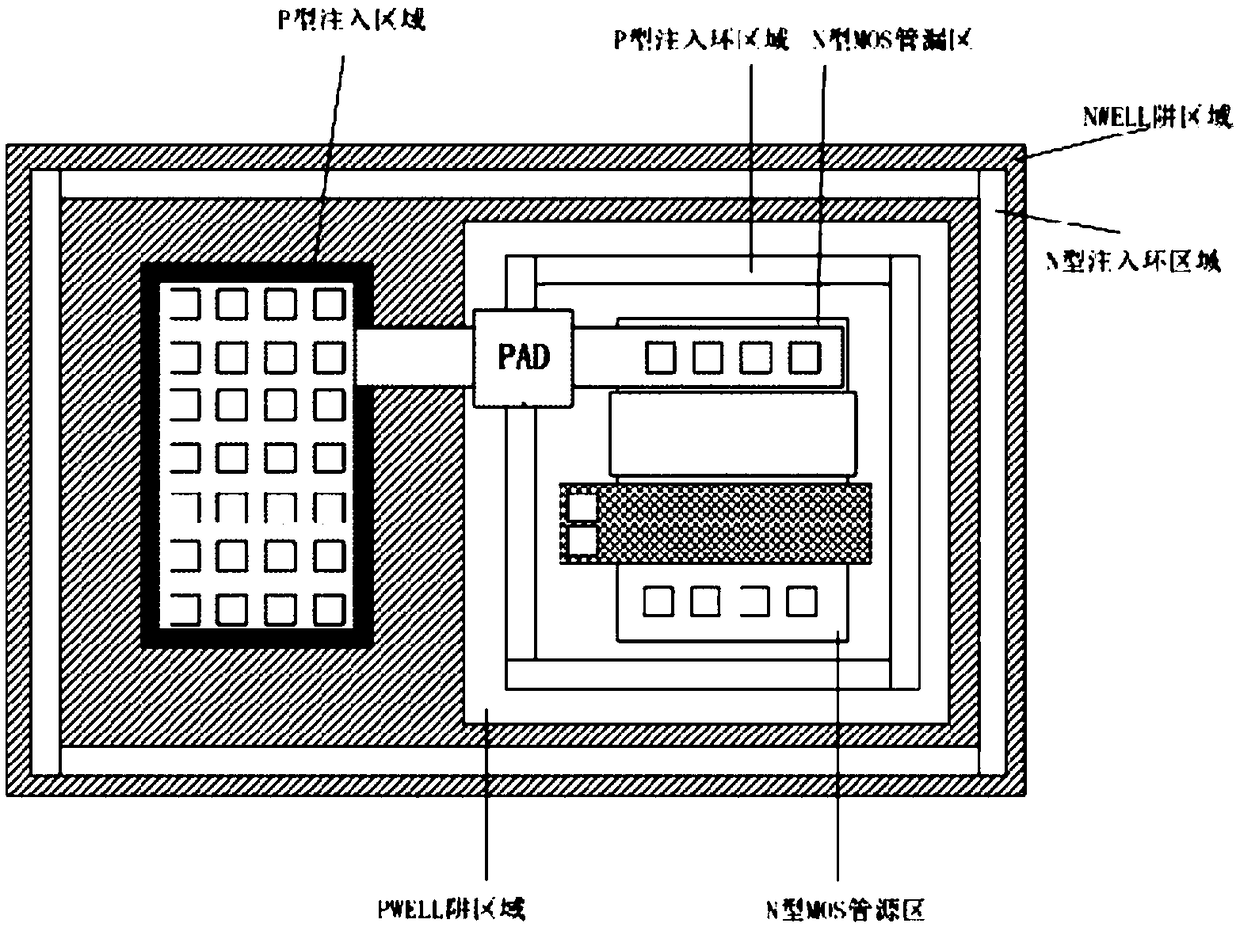
[0014] refer to figure 1 , an electrostatic discharge circuit provided by an embodiment of the present invention includes a PAD, a PN diode D1, a PN diode D2, an NPN transistor Q1, and an NPN transistor Q2; the anode of the PN diode D1, the cathode of the PN diode D2, the PAD and the NPN The collectors of the transistor Q1 and the NPN transistor Q2 are connected together, the cathode of the PN diode D1 and the emitter of the NPN transistor Q2 are both connected to the power supply terminal VCC, and the anode of the PN diode D2 and the cathode of the NPN transistor Q1 are commonly connected to Reference ground GND.

[0015] Specifically, PAD is a PCB pad, as a general term in this field; when positive static electricity occurs from PAD to the reference ground GND, since the direction of the positive and negative poles of PN diode D2 is opposite to the direction of the static electricity, the pad between the two The PN diode D2 is not conducting, but the NPN triode Q1 is forwar...


PUM


Abstract

The invention discloses an electrostatic discharge circuit and device. The electrostatic discharge circuit comprises PAD, a PN diode D1, a PN diode D2, an NPN triode Q1 and an NPN triode Q2, wherein apositive pole of the PN diode D1, a negative pole of the PN diode D2, the PAD and collectors of the NPN triode Q1 and the NPN triode Q2 are connected together; both a negative pole of the PN diode D1and an emitter of the NPN triode Q2 are connected to a power supply end VCC; and a positive pole of the PN diode D2 and a negative pole of the NPN triode Q1 are jointly connected to reference groundGND. Compared with the prior art, the electrostatic discharge circuit and device can realize negative charge release between a chip and the power supply end, thereby protecting the chip from being damages. Moreover, the electrostatic discharge circuit and device can be applied to a variety of different situations, and greatly improve the safety factor of the chip.

Description

technical field [0001] The invention relates to the field of semiconductor chips, in particular to an electrostatic discharge circuit and device. Background technique [0002] Static electricity exists on all kinds of circuit boards, and its instantaneous voltage is very high. Once it cannot be released to the outside, it is likely to burn the circuit components; at present, in the traditional static discharge circuit, when the chip When the negative charge discharge occurs between the power supply terminals, there is usually no direct discharge path, which makes the chip easy to be damaged. Contents of the invention [0003] In order to solve the above problems, the purpose of the embodiments of the present invention is to provide an electrostatic discharge circuit and device, which can realize negative charge discharge between the chip and the power supply terminal, thereby protecting the chip from damage. [0004] In order to make up for the deficiencies in the prior a...

Claims


Application Information

Patent Timeline
Patent Type & Authority Applications(China)
IPC IPC(8): H01L27/02
CPCH01L27/0255H01L27/0259H01L27/0292H01L27/0296
Inventor 张登军李建球安友伟余作欢杨小龙刘大海张亦锋李迪陈晓君逯钊琦
Owner 合肥博雅半导体有限公司
Why Eureka
Try Eureka