A capacitive fingerprint signal differential acquisition and amplification circuit and a working method thereof

A fingerprint signal and amplifying circuit technology, which is applied in printing image collection, acquisition/organization of fingerprints/palmprints, character and pattern recognition, etc., can solve problems such as flooding, destruction, and inability to obtain signal sensitivity and dynamic range, etc., to achieve reduction The effect of small distortion, high sensitivity and dynamic range

Active Publication Date: 2019-03-12
上海海栎创科技股份有限公司
View PDF5 Cites 0 Cited by
  • Summary
  • Abstract
  • Description
  • Claims
  • Application Information

AI Technical Summary

Problems solved by technology

The increase in the thickness of the insulating medium makes the effective fingerprint signal that can be collected become very small. On the one hand, it is easily overwhelmed by various DC signals on the chip, such as static leakage current, parasitic, etc.; This has become a major difficulty in the current design of capacitive fingerprint sensors. If this problem cannot be effectively solved, the signal sensitivity and dynamic range required to push the product to stable mass production cannot be obtained.

Method used


Image

  • A capacitive fingerprint signal differential acquisition and amplification circuit and a working method thereof
  • A capacitive fingerprint signal differential acquisition and amplification circuit and a working method thereof
  • A capacitive fingerprint signal differential acquisition and amplification circuit and a working method thereof

Examples


Embodiment Construction

[0030] The differential acquisition and amplification circuit of the capacitive fingerprint signal of the present invention and its working method will be described in more detail below in conjunction with the schematic diagram, wherein a preferred embodiment of the present invention is shown, and it should be understood that those skilled in the art can modify the present invention described here , while still realizing the advantageous effects of the present invention. Therefore, the following description should be understood as the broad knowledge of those skilled in the art, but not as a limitation of the present invention.

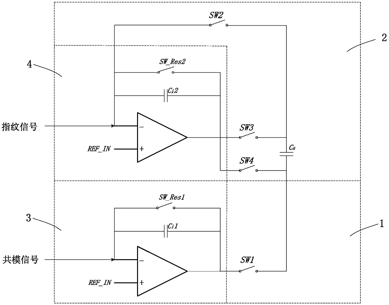
[0031] Please refer to figure 1 , in this embodiment, a differential acquisition and amplification circuit for capacitive fingerprint signals is proposed, a sampling array composed of at least one differential sampling channel 1 and a plurality of common sampling channels 2 .

[0032] Wherein, the differential sampling channel 1 includes a differenti...


PUM


Abstract

The invention provides a differential acquisition and amplification circuit of capacitive fingerprint signal and a working method thereof, By collecting the dc and ac components on the chip, The common-mode signal can be easily subtracted from the final signal before the second amplification, and the common-mode direct current component and the alternating current component in the original signalcan be effectively filtered out, so that a very high sensitivity and dynamic range can be obtained, and the differential-mode signal can be subsequently amplified by Cs / Ci times. At the same time, inthe second amplification stage, the distortion of the signal in the second amplification process can be minimized by matching the amplification capacitor Cs and the second integrating capacitor Ci2 onthe layout.

Description

technical field [0001] The invention relates to the technical field of integrated circuit design and fingerprint detection, in particular to a common-mode compensation and signal amplification circuit for small fingerprint signals. Background technique [0002] Due to its high reliability and cost-effectiveness, fingerprint authentication has become the mainstream of current biometric authentication; and capacitive fingerprint sensor is characterized by its small size, fast speed, low power consumption, high detection degree and great ease of use. , has become the mainstream method in fingerprint authentication, and has become the focus of current research. [0003] In the design of a capacitive fingerprint sensor, due to ESD and physical protection considerations, the thickness of the insulating medium on the fingerprint sensor is usually greater than 50 μm. The increase in the thickness of the insulating medium makes the effective fingerprint signal that can be collected ...

Claims


Application Information

Patent Timeline
IPC IPC(8): G06K9/00
CPCG06V40/1306
Inventor 朱定飞刘华王建军
Owner 上海海栎创科技股份有限公司
Why Eureka
Try Eureka