Gas inlet grid assembly and atomic layer deposition equipment

A technology for air intake grids and components, applied in coatings, gaseous chemical plating, metal material coating processes, etc., can solve problems such as abnormal discharge of power supply electrodes, abnormal film patterns, and abnormal patterns of films on the surface of wafers, so as to increase potential energy , Improve the stability and repeatability, the effect of good stability

Active Publication Date: 2019-03-19
BEIJING NAURA MICROELECTRONICS EQUIP CO LTD
View PDF10 Cites 7 Cited by
  • Summary
  • Abstract
  • Description
  • Claims
  • Application Information

AI Technical Summary

Problems solved by technology

[0005] In PEALD technology, during the high-power deposition process, the unstable gas pressure will cause abnormal discharge of the power supply electrode, resulting in abnormal patterns of the film on the wafer surface
Therefore, it is urgent to further improve the existing gas intake structure to solve the problem of abnormal film pattern caused by abnormal discharge.

Method used


Image

  • Gas inlet grid assembly and atomic layer deposition equipment
  • Gas inlet grid assembly and atomic layer deposition equipment
  • Gas inlet grid assembly and atomic layer deposition equipment

Examples


Embodiment Construction

[0076] Various embodiments of the invention will be described in more detail below with reference to the accompanying drawings. In the various drawings, the same elements are denoted by the same or similar reference numerals. For the sake of clarity, various parts in the drawings have not been drawn to scale.

[0077] The specific implementation manners of the present invention will be further described in detail below in conjunction with the accompanying drawings and embodiments.

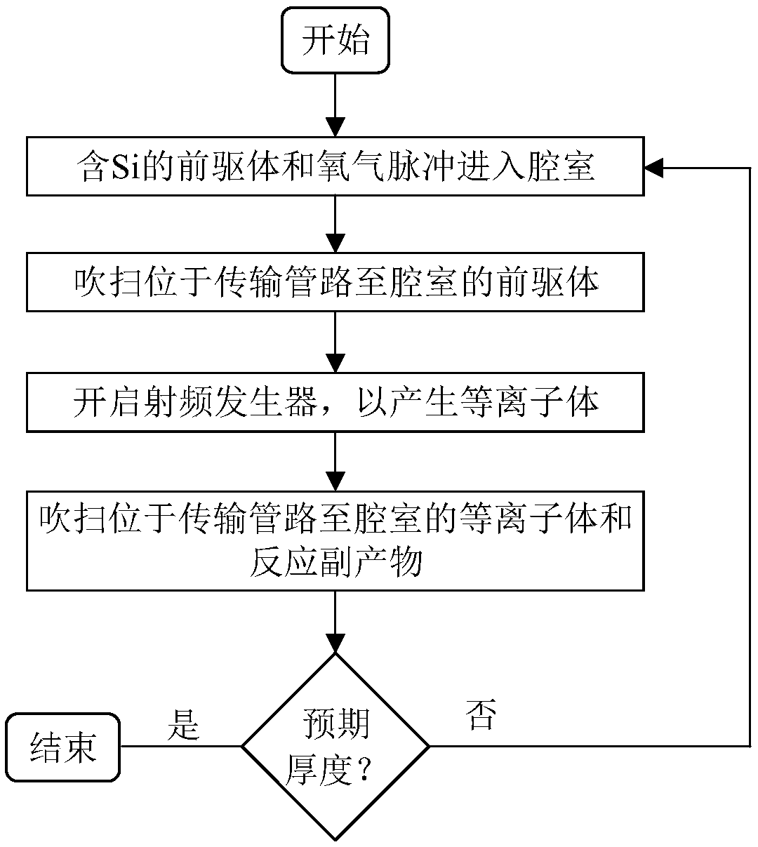
[0078] figure 1 A flow diagram of the plasma-enhanced atomic layer deposition technique is shown.

[0079] to deposit SiO 2 Thin film as an example, the existing PEALD deposited SiO 2 The deposition process of thin films generally uses Si-containing precursors and oxygen (O 2 ) scheme, the precursor (precursor) used is, for example, bis-diethylaminosilane (SAM24). Such as figure 1 As shown, in step S101, the Si-containing precursor and oxygen pulse enter the chamber until the substrate fully...


PUM

PropertyMeasurementUnit
lengthaaaaaaaaaa

Abstract

The invention discloses a gas inlet grid assembly and atomic layer deposition equipment. The gas inlet grid assembly comprises a first gas inlet grid, a second gas inlet grid and a cavity, wherein thefirst gas inlet grid comprises at least one gas outlet hole; the second gas inlet grid comprises at least one gas inlet hole; and the cavity is positioned between the first gas inlet grid and the second gas inlet grid, and communicates with the gas outlet hole and the gas inlet hole. By the adoption of the gas inlet grid assembly, the pressure intensity of gas in a gas inlet channel can be kept stable, the increased difficulty in controlling hollow cathode discharge due to the pressure intensity fluctuations can be avoided; and then the suppression of hollow cathode discharge can be facilitated.

Description

technical field [0001] The invention relates to the technical field of semiconductor manufacturing, in particular to an air inlet grid assembly and atomic layer deposition equipment. Background technique [0002] With the development of integrated circuit technology, the feature size of devices is gradually reduced, which puts forward higher requirements on the quality of deposited films, especially in three-dimensional device structures, such as Fin Field-Effect Transistor (Fin Field-Effect Transistor, FinFET), self- Aligned double imaging technology (Self to aligned to double to patterning, SADP) and three-dimensional flash memory (3D NAND) structure. Front-end-of-line (FEOL) thin films, such as oxides and nitrides, are facing challenges such as "device structure reduction requires more precise control of length and good film uniformity; more complex structures require required good conformality” and many other challenges. Traditional oxide deposition methods cannot meet...

Claims


Application Information

Patent Timeline
Patent Type & Authority Applications(China)
IPC IPC(8): C23C16/455
CPCC23C16/45544C23C16/45561
Inventor 秦海丰史小平兰云峰纪红赵雷超张文强
Owner BEIJING NAURA MICROELECTRONICS EQUIP CO LTD
Why Eureka
Try Eureka