

Spatial light modulator
An optical device and device technology, applied in the fields of instruments, optics, nonlinear optics, etc., can solve the problem of undisclosed optical device implementation methods, and achieve the effect of realizing phase modulation and improving response speed.
- Summary
- Abstract
- Description
- Claims
- Application Information
AI Technical Summary
Problems solved by technology
Method used
Image

Examples
Embodiment 1
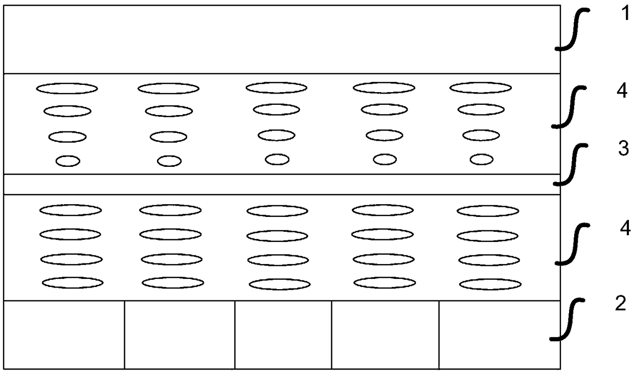
[0059] In one embodiment, the lower substrate uses a liquid crystal on silicon wafer with a resolution of 1920×1080, and both the intermediate dielectric layer and the upper substrate use ITO glass. The liquid crystal is selected as the upper liquid crystal is packaged in TN mode, and the lower layer is packaged in ECB mode. A possible alignment selection is that both the surface of the lower substrate and the surface of the intermediate dielectric layer are aligned at 45° to one side of the device, and the surface of the upper substrate is aligned parallel or perpendicular to one side of the device. The distance between the upper substrate and the ITO glass is 1um (that is, the thickness of the upper liquid crystal layer is 1um), and the distance between the ITO glass and the lower substrate is 2.5um (that is, the thickness of the lower liquid crystal layer is 2.5um).
[0060] The light source (pixel) uses an OLED display panel, and a polarizing prism is added to the light pa...
Embodiment 2
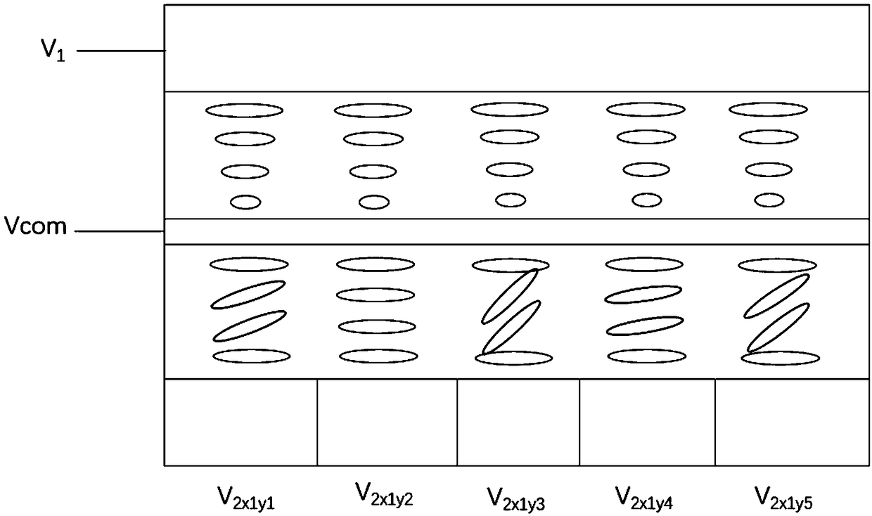
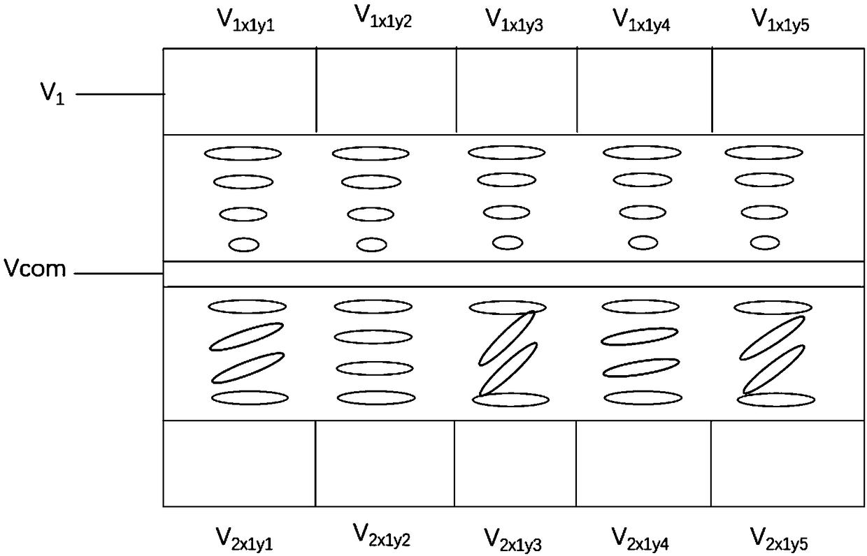
[0068] In Embodiment 2, both the upper substrate and the lower substrate are made of transparent materials, and both the upper substrate and the lower substrate are TFT substrates with pixel point voltage modulation capabilities. The alignment direction of the substrate is consistent with the surface of the corresponding dielectric layer, and it is consistent with the alignment direction of the upper substrate or one of the surfaces of the dielectric layer corresponding to the upper substrate. The polarization direction of the light emitted by the light source is changed after passing through the upper substrate. The amount is determined by the input signal of each pixel. The same as the above example, the polarization direction of all pixels can be equivalently decomposed into a combination of the direction consistent with the alignment direction of the underlying substrate and the direction perpendicular to the alignment direction of the underlying substrate, because the long...
Embodiment 3
[0070] Another application is to reduce the required thickness of a single-layer material by laminating multiple layers of birefringent materials (thickness and response time are generally in a quadratic relationship, the smaller the thickness, the faster the response speed of the material), so as to achieve the same phase and / or within the range of intensity modulation, improving the response time of the device itself. For example, in Embodiment 3, the optical device includes a multilayer structure (comprising three layers of birefringent materials), the lower substrate uses a silicon-based liquid crystal wafer, and a conductive medium layer is 1.8um away from the wafer, and the two surfaces of the conductive medium layer The alignment direction of the substrate is the same as that of the lower substrate, and the liquid crystal material is filled between the two layers. The conductive medium layer is at least 1.8um and is a transparent intermediate substrate, on which electr...
PUM
 Abstract
Description
Claims
Application Information