

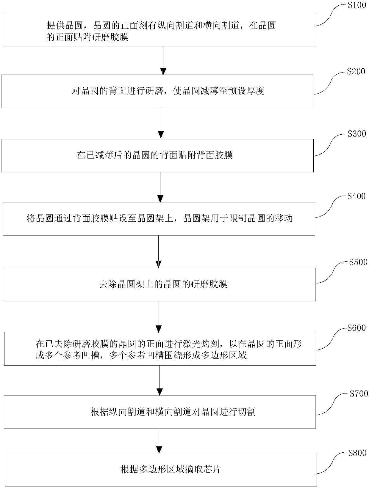
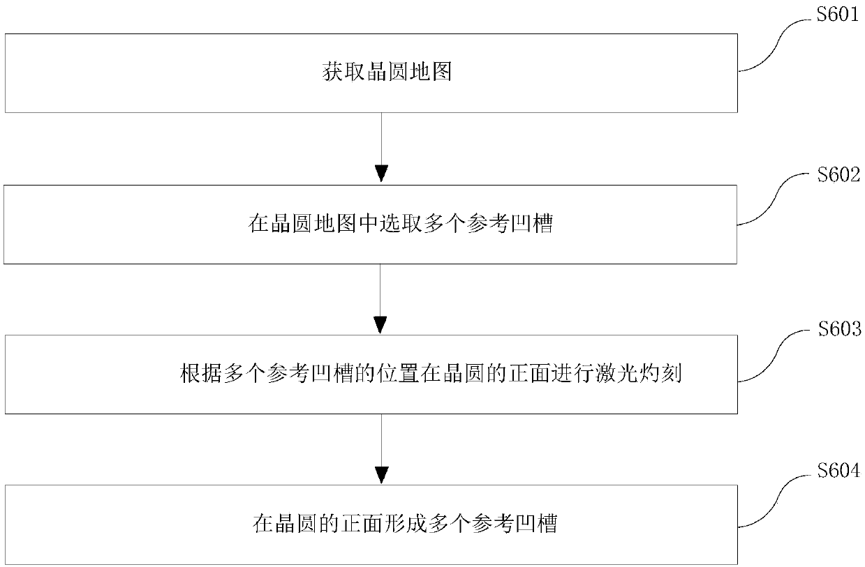
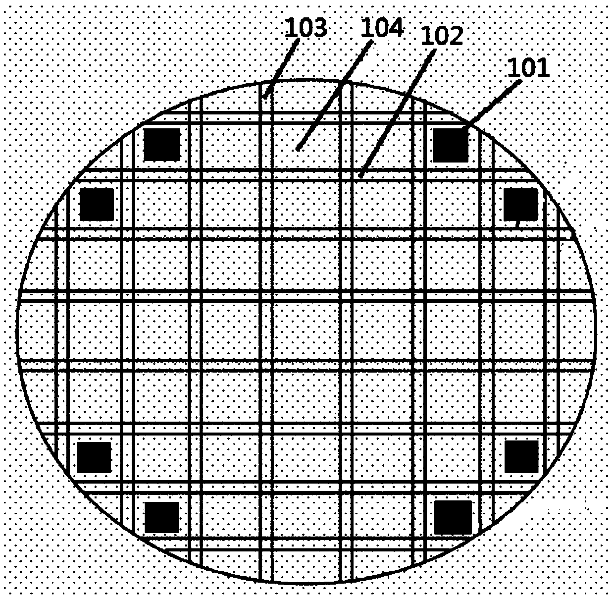
Wafer cutting process
A cutting process and wafer technology, applied in manufacturing tools, metal processing equipment, laser welding equipment, etc., can solve problems such as difficult identification of reference points, doping of unqualified chip products, etc.
- Summary
- Abstract
- Description
- Claims
- Application Information
AI Technical Summary
Problems solved by technology
Method used
Image

Examples
Embodiment Construction
[0036] In order to make the purpose, technical solutions and advantages of the embodiments of the present invention clearer, the technical solutions in the embodiments of the present invention will be clearly and completely described below in conjunction with the drawings in the embodiments of the present invention. Obviously, the described embodiments It is a part of embodiments of the present invention, but not all embodiments. Based on the embodiments of the present invention, all other embodiments obtained by persons of ordinary skill in the art without creative efforts fall within the protection scope of the present invention.
[0037] In describing the present invention, it should be understood that the terms "center", "longitudinal", "transverse", "upper", "lower", "front", "rear", "left", "right", " The orientations or positional relationships indicated by "vertical", "horizontal", "top", "bottom", "inner", "outer", "axial", "radial", and "circumferential" are based on...
PUM
| Property | Measurement | Unit |
|---|---|---|
| Depth | aaaaa | aaaaa |
| Thickness | aaaaa | aaaaa |
Abstract
Description
Claims
Application Information