
Semiconductor device and method of making the same

A manufacturing method and semiconductor technology, applied in the direction of semiconductor devices, electrical solid devices, electrical components, etc., can solve the problems of polysilicon layer etching process influence, step height difference, affecting device performance, etc., to achieve effective integration and step height The effect of reduced differences and effective integration

Inactive Publication Date: 2019-03-29
WUHAN XINXIN SEMICON MFG CO LTD
View PDF4 Cites 1 Cited by
  • Summary
  • Abstract
  • Description
  • Claims
  • Application Information

AI Technical Summary

Problems solved by technology

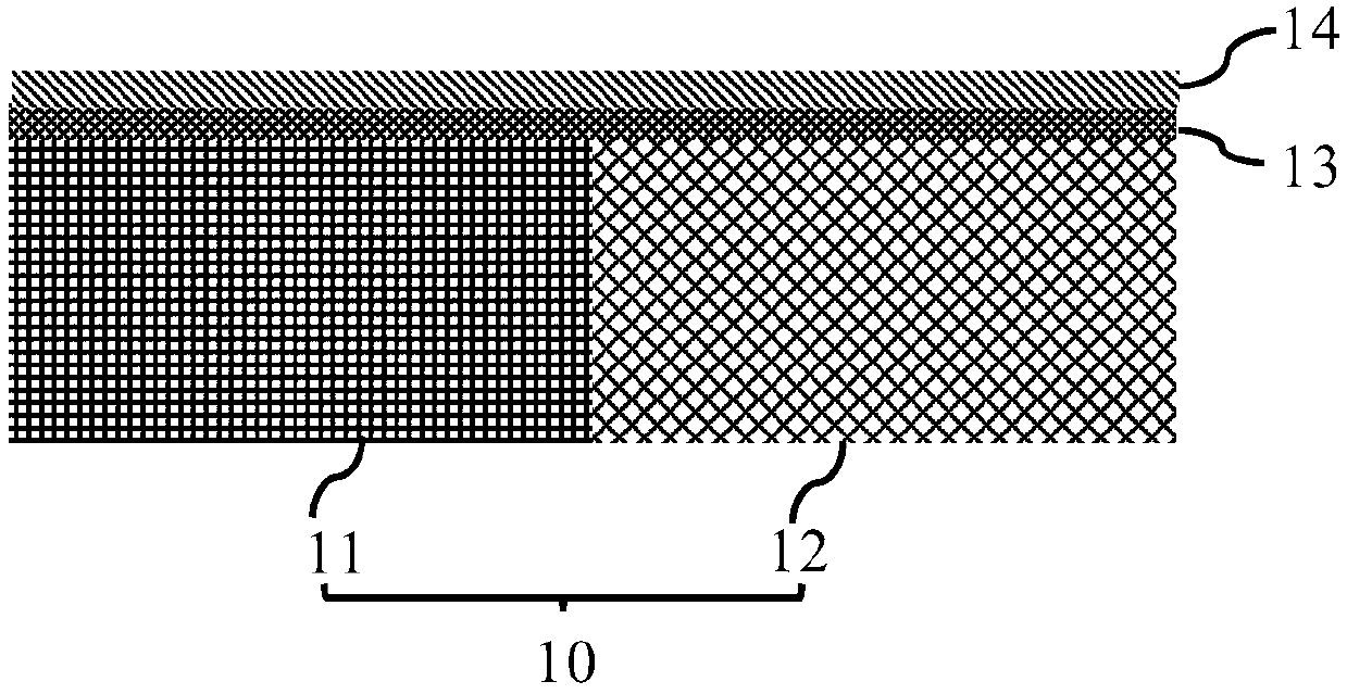
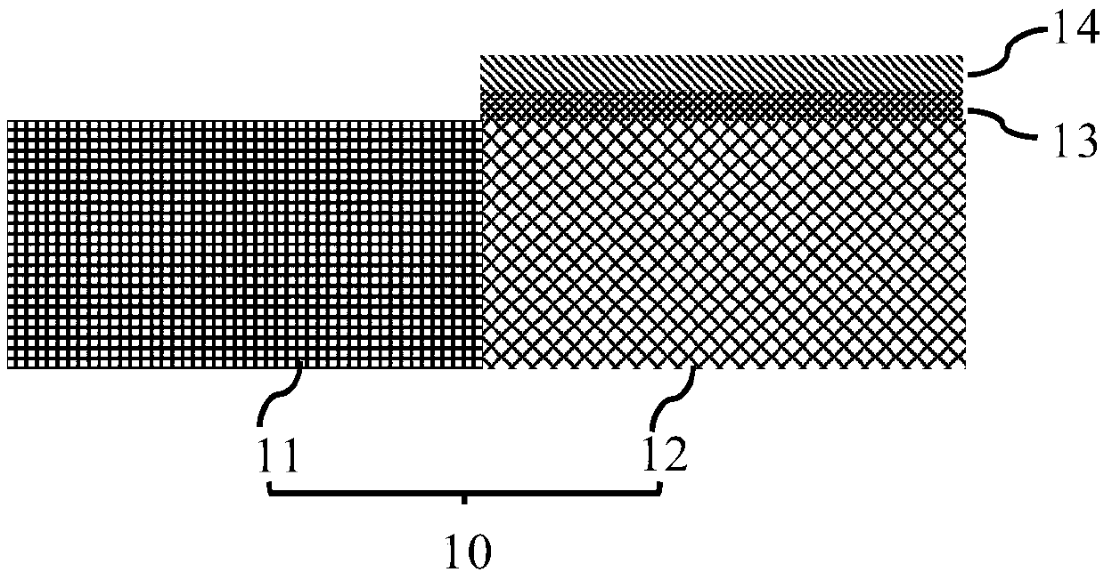
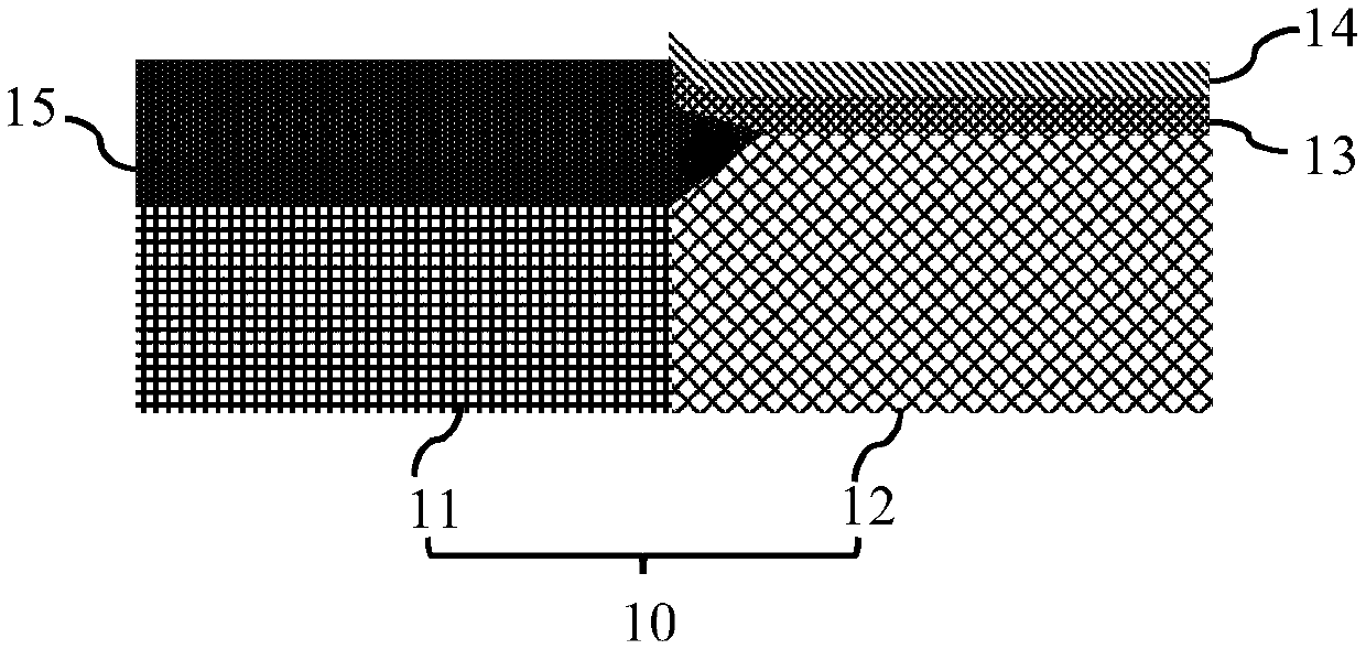
[0008] The first gate oxide layer 15 is very thick, and the second gate oxide layer 17 is relatively thin, so that the first gate oxide layer 15 on the high-voltage device region 11 and the second gate oxide layer on the low-voltage device region 12 formed by the above prior art There is a large height difference on the top surface of 17, resulting in a large difference in the height of the steps formed between the first gate oxide layer 15 and the second gate oxide layer 17 and the shallow trench isolation structure 16, which in turn affects the subsequent process. , such as affecting the etching process of the polysilicon layer
like Figure 1e As shown in , if the step height H1 formed by the first gate oxide layer 15 and the shallow trench isolation structure 16 is The step height H2 formed by the second gate oxide layer 17 and the shallow trench isolation structure 16 is During the subsequent etching of the polysilicon layer formed on the high-voltage device region 11 and the low-voltage device region 12, the polysilicon on the sidewall of the shallow trench isolation structure 16 located on the low-voltage device region 12 cannot be etched clean, affecting the device. performance

Method used


Image

  • Semiconductor device and method of making the same
  • Semiconductor device and method of making the same
  • Semiconductor device and method of making the same

Examples


Embodiment Construction

[0042] In order to make the purpose, advantages and characteristics of the present invention clearer, the following in conjunction with the attached Figure 2~3I The semiconductor device proposed by the present invention and its manufacturing method are further described in detail. It should be noted that all the drawings are in a very simplified form and use imprecise scales, and are only used to facilitate and clearly assist the purpose of illustrating the embodiments of the present invention.

[0043] An embodiment of the present invention provides a method for manufacturing a semiconductor device, see figure 2 , figure 2 It is a flowchart of a method for manufacturing a semiconductor device according to an embodiment of the present invention, and the method for manufacturing a semiconductor device includes:

[0044] Step S2-A, providing a substrate having a high-voltage device region and a low-voltage device region;

[0045] Step S2-B, etching and removing a part of t...


PUM


Abstract

The invention provides a semiconductor device and a method of making the same. The method comprises: providing a substrate having a high-voltage device region and a low-voltage device region; carryingout etching to remove the substrate with the partial thickness in the high-voltage device region and thus forming a first trench in the high-voltage device region; forming a first gate oxide layer inthe first trench; forming a shallow trench isolation structure at a junction of the high-voltage device region and the low-voltage device region; and forming a second gate oxide layer on the low-voltage device region. Therefore, when the thickness of the first gate oxide layer meets the high operating voltage, the difference between the step heights formed by the first gate oxide layer and the shallow trench isolation structure and between the second gate oxide layer and the shallow trench isolation structure is reduced to avoid the influence on the follow-up process; and thus effective integration of a high-voltage device and a low-voltage device is realized.

Description

technical field [0001] The invention relates to the field of semiconductor integrated circuit manufacturing, in particular to a semiconductor device and a manufacturing method thereof. Background technique [0002] In the field of semiconductor integrated circuits, high-voltage devices are necessary devices in many circuits, such as storage circuits, and circuits also require faster low-voltage devices to complete logic processing. In order to achieve a higher operating voltage for high-voltage devices, the thickness of the gate oxide layer on the high-voltage device is generally very thick. At the same time, for low-voltage devices to achieve a faster speed, a thinner gate oxide layer is required. In the prior art, the steps of forming a gate oxide layer on high-voltage devices and low-voltage devices are generally: [0003] 1. First, a pad oxide layer 13 and a silicon nitride layer 14 are formed on a substrate 10 having a high-voltage device region 11 and a low-voltage de...

Claims


Application Information

Patent Timeline
Patent Type & Authority Applications(China)
IPC IPC(8): H01L27/115H01L27/11568H01L29/06H10B69/00H10B43/30
CPCH01L29/0642H01L29/0684H10B69/00H10B43/30
Inventor 赵东光
Owner WUHAN XINXIN SEMICON MFG CO LTD
Learn More