A terahertz wave photonic crystal device with real-time adjustable response frequency band and its preparation method and application

A photonic crystal and terahertz wave technology, applied in the field of terahertz wave applications, can solve problems such as unfavorable technical barriers, elimination, and single working frequency band

Active Publication Date: 2020-11-27
INST OF METAL RESEARCH - CHINESE ACAD OF SCI
View PDF3 Cites 0 Cited by
  • Summary
  • Abstract
  • Description
  • Claims
  • Application Information

AI Technical Summary

Problems solved by technology

However, this frequency band is mostly concentrated in the GHz frequency band. The application of this frequency band is mature, and the technical barriers are disappearing day by day. Existing research shows that in the future, the technological competition in this field will shift from the GHz field to the terahertz frequency field, which will lead to traditional stealth materials. failure and elimination
In addition, the existing stealth materials have the inherent defects of single working frequency band and non-adjustable working frequency band, which is not conducive to the establishment of technical barriers. Now the development of this technology is hindered.

Method used


Image

  • A terahertz wave photonic crystal device with real-time adjustable response frequency band and its preparation method and application
  • A terahertz wave photonic crystal device with real-time adjustable response frequency band and its preparation method and application

Examples


Embodiment 1

[0024] The process of preparing a terahertz photonic crystal device in this embodiment is as follows:

[0025] Step 1: Add 5g of iron powder into 5g of Dow Corning SE1700, and mix evenly to obtain the magnetic ink to be printed.

[0026] Step 2, the ink is loaded into the printer barrel, the pitch of the close-packed structure is set to 500 microns, and the layer height is 150 microns, and the photonic crystal structure is printed according to the three-dimensional wood stack structure array.

[0027] In step 3, the printed photonic crystal three-dimensional array is heated and cured at 100° C. for 1 hour.

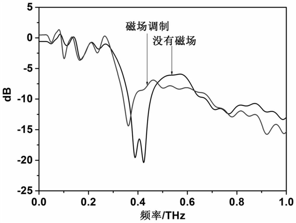
[0028] Step 4, conduct a terahertz spectrum test on the heat-treated terahertz photonic crystal stealth device, and obtain the photonic band gap through Fourier transform, and the result is in figure 1 displayed in (no magnetic field).

[0029] Step 5: Modulate the terahertz photonic crystal cloaking device with an external magnetic field, and at the same time perform te...

Embodiment 2

[0031] The process of preparing a terahertz photonic crystal device in this embodiment is as follows:

[0032] Step 1: Add 5g of iron powder into 5g of Dow Corning SE1700, and mix evenly to obtain the magnetic ink to be printed.

[0033] Step 2, the ink is loaded into the printer barrel, the pitch of the close-packed structure is set to 400 microns, and the layer height is 150 microns, and the photonic crystal structure is printed according to the three-dimensional wood stack structure array.

[0034] In step 3, the printed photonic crystal three-dimensional array is heated and cured at 100° C. for 2 hours.

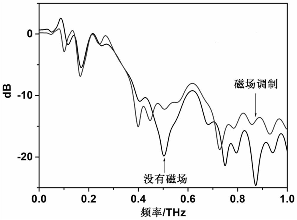
[0035] Step 4, conduct a terahertz spectrum test on the heat-treated terahertz photonic crystal stealth device, and obtain the photonic band gap through Fourier transform, and the result is in figure 2 displayed in (no magnetic field).

[0036] Step 5: Add magnetic field modulation to the terahertz photonic crystal stealth device, and perform terahertz time-domain spec...


PUM


Abstract

The invention discloses a terahertz wave photonic crystal device with a real-time adjustable response frequency band and a preparation method and application thereof, and belongs to the technical field of terahertz wave application and 3D printing. According to the terahertz wave photonic crystal device, a high-permeability magnetic material and a flexible material are combined to realize a photonic crystal three-dimensional array through a module-free direct-writing three-dimensional printing technology; the three-dimensional array with different geometric periodic structures and powder materials therein can cooperate with each other to absorb terahertz waves with different frequency bands; and response, to external magnetic fields, of the magnetic material is utilized to further change three-dimensional periodic structures of photonic crystal invisible devices. The photonic crystal device can be used as an adjustable optical window to realize invisibility and modulation of terahertzwaves with different frequency bands, and can be used as a detector to sense changes of external magnetic fields in spaces where the devices are located.

Description

Technical field: [0001] The invention relates to the fields of terahertz wave application technology and 3D printing technology, in particular to a terahertz wave photonic crystal device with a real-time adjustable response frequency band and its preparation method and application. Background technique: [0002] Photonic crystals refer to a class of materials designed to have a certain periodic structure in order to achieve a certain electromagnetic field response. In the field of electromagnetic wave stealth, when the electromagnetic wave is incident on the photonic crystal, due to the special space array structure of the photonic crystal, the photon band gap is caused. In the photon band gap, the photon density of state disappears, resulting in the inability of the electromagnetic wave to propagate. stealth. [0003] Traditional stealth materials (including existing stealth materials based on photonic crystal theory), such as stealth coatings for stealth fighters, are des...

Claims


Application Information

Patent Timeline
Patent Type & Authority Patents(China)
IPC IPC(8): G02F1/00G02B6/122
CPCG02B6/1225G02F1/0063G02F1/0081
Inventor 李琦杨炜沂朱朋飞王荣鞠小晶
Owner INST OF METAL RESEARCH - CHINESE ACAD OF SCI
Why Eureka
Try Eureka