Image sensor and formation method thereof

A technology of image sensors and switching devices, applied in the direction of electric solid-state devices, semiconductor devices, electrical components, etc., can solve problems such as image smearing, image influence, photogenerated carrier photoelectric conversion layer residue, etc., to reduce the possibility and improve quality, image quality enhancement effects

Inactive Publication Date: 2019-04-02
HUAIAN IMAGING DEVICE MFGR CORP
View PDF3 Cites 2 Cited by
  • Summary
  • Abstract
  • Description
  • Claims
  • Application Information

AI Technical Summary

Problems solved by technology

[0005] However, in the above-mentioned image sensor, the photogenerated carriers need to travel a long path to be transported to the logic device, and it is easy to cause the problem that the photogenerated

Method used


Image

  • Image sensor and formation method thereof
  • Image sensor and formation method thereof
  • Image sensor and formation method thereof

Examples


Embodiment Construction

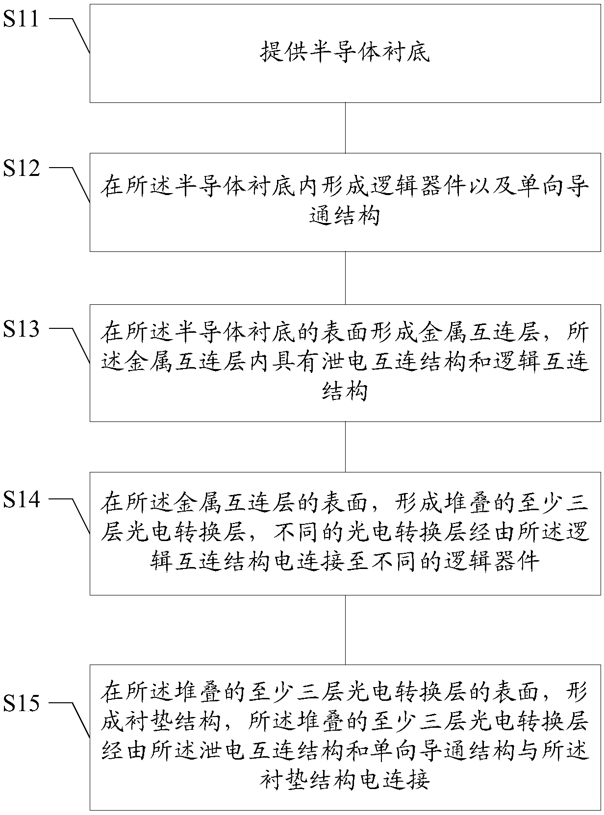
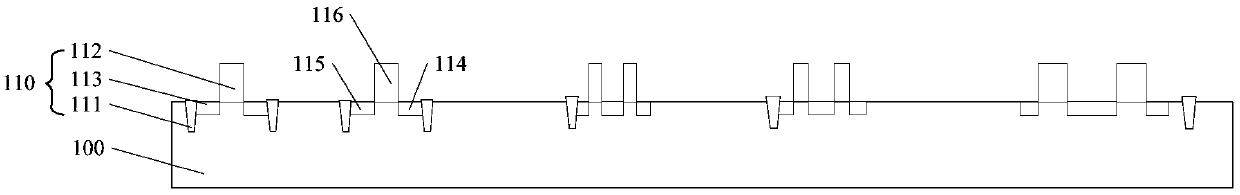
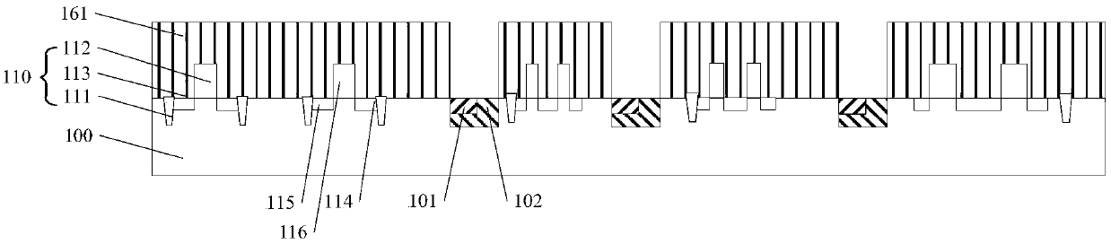
[0026] As mentioned above, in an image sensor, stacked photoelectric conversion layers are used to generate photo-generated carriers, and then the photo-generated carriers are transported to the logic device through the conductive structure and the metal interconnection structure, but it is easy to occur Image smearing problem.

[0027] The inventors of the present invention have found through research that, in the above-mentioned image sensor, the photogenerated carriers need to pass through the photoelectric conversion layer, the dielectric layer, the conduction structure, the metal interconnection structure, etc. to the logic device, and the moving path is relatively long. It is prone to the problem that the photogenerated carriers generated during the previous illumination remain in the photoelectric conversion layer, which will affect the image formed by the subsequent illumination and cause image smearing.

[0028] In the embodiment of the present invention, by forming a...


PUM


Abstract

Disclosed are an image sensor and a formation method thereof. The image sensor comprises a semiconductor substrate, a metal interconnection layer, at least three layers of stacked photoelectric conversion layers, and a liner structure, wherein logic devices and a unidirectional conduction structure are formed in the semiconductor substrate; the metal interconnection layer is located on the surfaceof the semiconductor substrate, wherein a drain interconnection structure and a logic interconnection structure are arranged in the metal interconnection layer; the at least three layers of stacked photoelectric conversion layers are located on the surface of the metal interconnection layer, wherein the different photoelectric conversion layers are electrically connected to different logic devices through the logic interconnection structure; and the liner structure which is positioned on the surfaces of at least three layers of stacked photoelectric conversion layers, wherein the at least three layers of stacked photoelectric conversion layers are electrically connected with the liner structure through the drain interconnection structure and the unidirectional conduction structure. By virtue of the scheme, photon-generated carriers in the photoelectric conversion layers can be guided out, so that the possibility of image streaking is lowered.

Description

technical field [0001] The invention relates to the technical field of semiconductor manufacturing, in particular to an image sensor and a forming method thereof. Background technique [0002] The image sensor is the core component of the camera equipment, which realizes the image capture function by converting the optical signal into an electrical signal. Taking a CMOS image sensor (CMOS Image Sensors, CIS) device as an example, due to its advantages of low power consumption and high signal-to-noise ratio, it has been widely used in various fields. [0003] However, in the prior art, the ion implantation process is used to form the photodiode (PhotoDiode, PD) in the pixel device, which is easy to cause damage to the semiconductor substrate, and the size of the manual pixel device is limited, and the size of the photodiode is often small, resulting in There are fewer photogenerated carriers; and in the process of forming the optical filter matrix, the production cost is rel...

Claims


Application Information

Patent Timeline
IPC IPC(8): H01L27/146
CPCH01L27/14605H01L27/1461H01L27/14636H01L27/14687H01L27/14692
Inventor 吴明吴孝哲林宗贤吴龙江熊建锋朱晓彤
Owner HUAIAN IMAGING DEVICE MFGR CORP
Why Eureka
Try Eureka