Semiconductor laser spectrum combining and frequency multiplication device

A spectral beam combining and semiconductor technology, which is applied in the field of semiconductor laser spectral beam combining and frequency doubling devices, can solve the problems of reducing efficiency, loss, limited improvement of power and brightness, etc.

Pending Publication Date: 2019-04-02
FUZHOU PHOTOP QPTICS CO LTD
View PDF0 Cites 5 Cited by
  • Summary
  • Abstract
  • Description
  • Claims
  • Application Information

AI Technical Summary

Problems solved by technology

Polarization beam combining combines the light of two polarization directions into one beam through polarization-related devices, and the brightness can only be doubled. It is generally used in conjunction with other beam combining technologies; wavelength beam combining is limited by coating technology, and the number of beam combining units generally does not exceed 5, the improvement of power and brightness is also limited; there is a limit to the NA of the laser beam combined by fiber optics, and the combination of multiple laser beams will reduce the efficiency and there is a certain loss in the fiber coupling process

Method used


Image

  • Semiconductor laser spectrum combining and frequency multiplication device
  • Semiconductor laser spectrum combining and frequency multiplication device
  • Semiconductor laser spectrum combining and frequency multiplication device

Examples


Embodiment Construction

[0025] Example embodiments will now be described more fully with reference to the accompanying drawings. Example embodiments may, however, be embodied in many forms and should not be construed as limited to the embodiments set forth herein. Rather, these embodiments are provided so that this application will be thorough and complete, and will fully convey the concept of the example embodiments to those skilled in the art. The same reference numerals denote the same or similar structures in the drawings, and thus their repeated descriptions will be omitted.

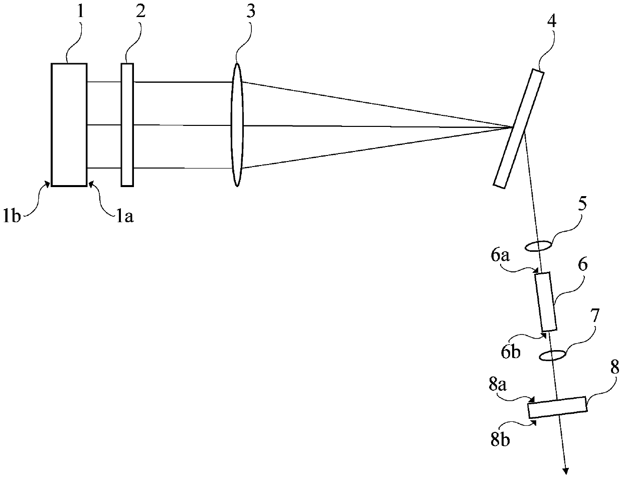
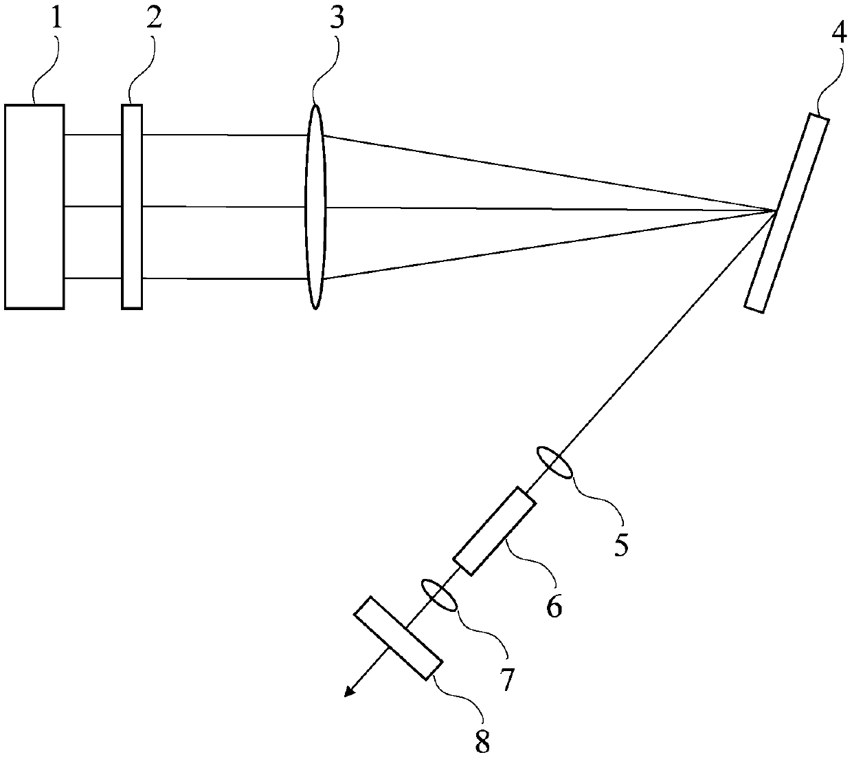
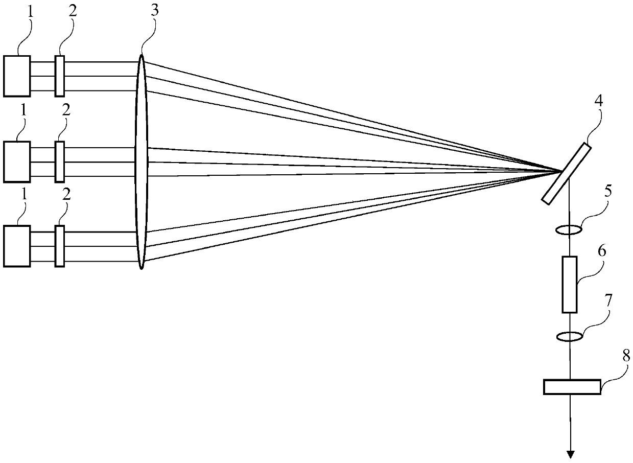
[0026] Figure 1 to Figure 3 A schematic diagram of three kinds of semiconductor laser spectral beam combining and frequency doubling devices in the embodiment is shown. combine Figure 1 to Figure 3 As shown, in some embodiments of the present application, the semiconductor laser spectrum combining beam frequency doubling device includes:

[0027] A semiconductor laser 1 for emitting multiple parallel beams, a convers...


PUM


Abstract

The present application provides a semiconductor laser spectrum combining and frequency multiplication device and relates to the field of laser devices. The semiconductor laser spectrum combining andfrequency multiplication device comprises a semiconductor laser, a conversion lens, a diffraction grating, a frequency multiplication crystal and an output coupling mirror which are arranged successively, wherein the semiconductor laser is located at the front focal plane of the conversion lens; the center of the diffraction grating coincides with the back focus of the conversion lens; the multiple parallel beams emitted by the semiconductor laser are focused to the diffraction grating by the conversion lens, and coupled by the diffraction grating into combined light to be output; the output coupling mirror reflects the fundamental-frequency light, and increases the permeability of the frequency-multiplied light. The combined light output by the diffraction grating is subjected to the frequency multiplication of the frequency multiplication crystal and is output by the output coupling mirror. The device achieves spectrum combining by the diffraction grating, increases output power andbrightness, and the power density and conversion efficiency of the laser in the frequency multiplication crystal, and reflects the fundamental-frequency light and increases the permeability of the frequency-multiplied light by the output coupling mirror to obtain high-power and high-efficiency frequency-multiplied laser output.

Description

technical field [0001] The present application relates to the field of laser equipment, in particular, to a semiconductor laser spectrum combining beam frequency doubling device. Background technique [0002] Semiconductor lasers have the advantages of low cost, long life, small size, and high reliability. They have broad application prospects in industrial processing, pumping, medical treatment, and communications. Whether the brightness of semiconductor lasers can be further improved is an important factor restricting the future development of semiconductor lasers. The brightness of the laser beam is determined by the output power and beam quality. The higher the power, the better the beam quality and the higher the brightness. The application fields of semiconductor lasers are also wider. In addition, for some specific wavelength semiconductor lasers, the output power is limited and the price is very high; and due to the limitations of current semiconductor technology, f...

Claims


Application Information

Patent Timeline
Patent Type & Authority Applications(China)
IPC IPC(8): H01S5/06
CPCH01S5/06H01S5/0605
Inventor 赵明周权丁永奎
Owner FUZHOU PHOTOP QPTICS CO LTD
Why Eureka
Try Eureka