Fabrication method of printed circuit board

A technology for printed circuit boards and manufacturing methods, which is applied in the fields of printed circuit manufacturing, printed circuits, printed circuit components, etc., and can solve problems such as difficult design of positioning holes on the board, deviation of the shape of the circuit board, and difficulty in fixing small-sized circuit boards. Achieve the effects of improving inspection efficiency and accuracy, improving production efficiency and pass rate, and reducing the number of scratches

Inactive Publication Date: 2019-04-02
江门市利诺达电路科技有限公司
View PDF6 Cites 3 Cited by
  • Summary
  • Abstract
  • Description
  • Claims
  • Application Information

AI Technical Summary

Problems solved by technology

[0003] In the prior art, the shape of the small-sized circuit board is processed by milling machine technology. However, due to the small area of ​​the small-sized circuit board, it is difficult to design positioning holes in the board, which makes it difficult to fix the small-sized circuit board during the process of shape processing, resulting in Problems such as deviation and breakage of the circuit board shape; moreover, when the size of the circuit board is smaller than the dust collection device of the processing equipment, the circuit board is easily sucked and lost by the dust collection device during processing; in addition, for small-sized circuit boards During the inspection, due to the small size of the board, it is inconvenient for the inspector to take it, which reduces the inspection efficiency. Moreover, during the inspection process, the hand of the inspector easily blocks the inspection position of the board, resulting in the outflow of the problem board

Method used


Image

  • Fabrication method of printed circuit board
  • Fabrication method of printed circuit board
  • Fabrication method of printed circuit board

Examples


Embodiment Construction

[0032] The following will clearly and completely describe the technical solutions in the embodiments of the present invention with reference to the accompanying drawings in the embodiments of the present invention. Obviously, the described embodiments are only some, not all, embodiments of the present invention. Based on the embodiments of the present invention, all other embodiments obtained by persons of ordinary skill in the art without creative efforts fall within the protection scope of the present invention.

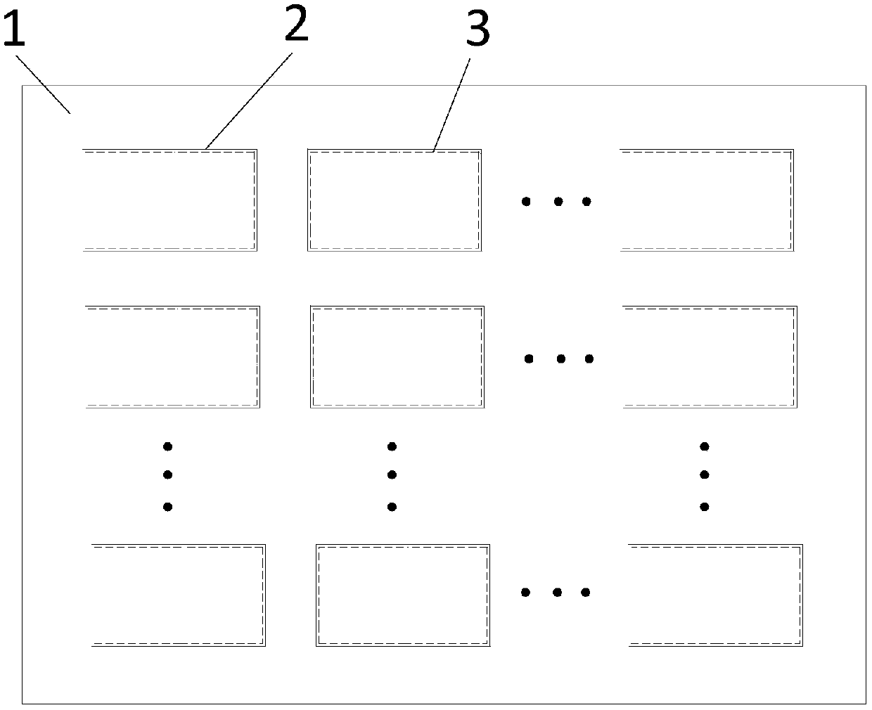
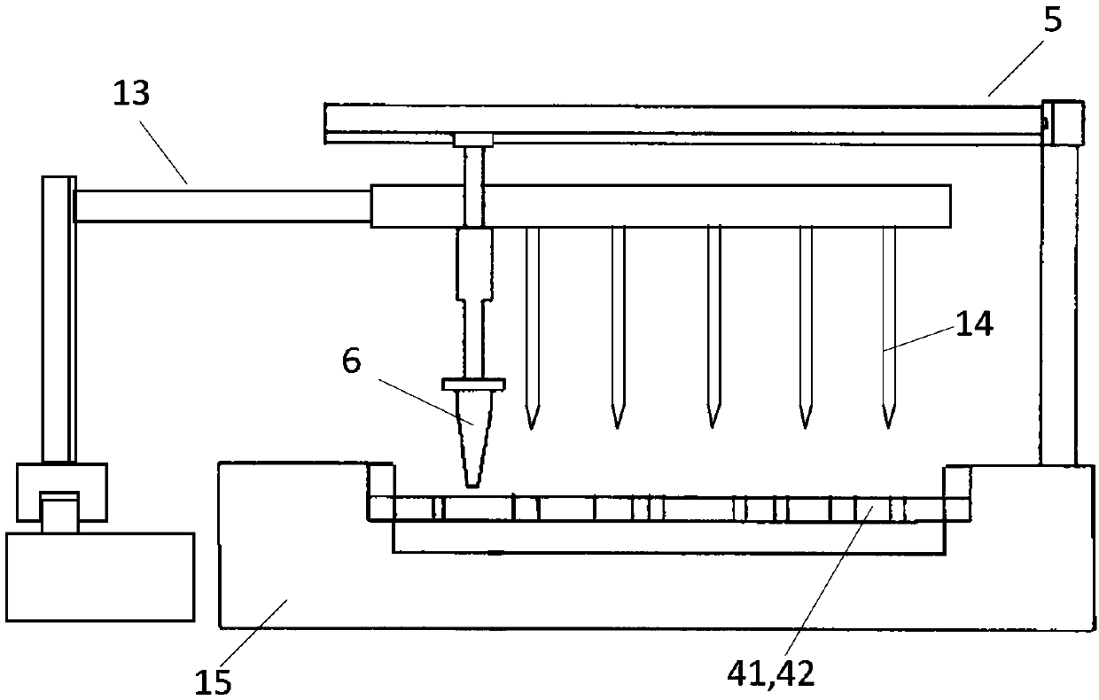
[0033] Such as Figure 1 to Figure 3 As shown, the preferred embodiment of the present invention, a method of manufacturing a printed circuit board, includes the following processes: material cutting, drilling, copper sinking, pattern transfer, pattern electroplating, film removal, etching, green oil, characters, gold-plated fingers , molding and testing, it is characterized in that, the specific steps of described molding and described testing are as follows:

[...


PUM


Abstract

The invention provides a fabrication method of a printed circuit board. By designing a partition line during the formation step, the circuit board can be still connected with a plate after cutting andformation, particularly for fabrication of a small-size circuit board, a positioning hole is not needed to be formed in each circuit board, the appearance damage of the circuit board is reduced, andthe production efficiency and the qualified size of the circuit board are improved; in the detection step, the quality of a via hole, such as hole position and hole plug state can be judged by comparing difference between reflection intensity, detected by an infrared emission sensor, of an infrared ray after passing through a standard hole and a to-be-measured hole; and the quality of each loop ofthe circuit board is detected one by one, and the short-circuit condition of each loop of a to-be-detected circuit board is judged by comparing difference between inductance values, detected by a probe, of each loop of a standard circuit board and each loop of a to-be-detected circuit. The fabrication method has the advantages of high production rate, high detection efficiency, high detection accuracy and high cleaning efficiency and is convenient to process.

Description

technical field [0001] The invention relates to the technical field of printed circuit boards, in particular to a method for manufacturing a printed circuit board. Background technique [0002] With the development of circuit boards in the direction of small size, light weight, three-dimensional installation and high connection reliability, there are more and more small-sized circuit boards in the printed circuit board industry. Shape processing and finished product inspection are essential in the process of circuit board production. There are two least processes, among which, the shape processing is specifically to use the shape processing equipment (such as punching machine, edge milling machine) to process the imposition products into the single board form or delivery panel form required by the customer; the finished product inspection is specifically the finished circuit Before the board is shipped, use the naked eye or borrow tools (such as a magnifying glass, etc.) to ...

Claims


Application Information

Patent Timeline
Patent Type & Authority Applications(China)
IPC IPC(8): H05K3/00H05K1/02
CPCH05K1/0268H05K1/0269H05K3/00H05K3/0044
Inventor 童雷童炳武童大望潘世丹
Owner 江门市利诺达电路科技有限公司
Why Eureka
Try Eureka