Unlock instant, AI-driven research and patent intelligence for your innovation.

PCB (Printed Circuit Board)-oriented printing control method and device, and storage medium

A PCB board, printing control technology, applied in printing devices, printing, typewriters, etc., can solve the problems of long cycle, complex printing process, low efficiency, etc., and achieve the effect of high precision, accurate pattern and high efficiency

Active Publication Date: 2019-04-02
SHENZHEN HOSONSOFT CO LTD
View PDF7 Cites 7 Cited by
  • Summary
  • Abstract
  • Description
  • Claims
  • Application Information

AI Technical Summary

Problems solved by technology

[0005] The main purpose of the present invention is to propose a printing control method, device and storage medium for PCB boards, aiming to solve the technical problems of complicated printing process, long cycle and low efficiency of the existing PCB board circuit

Method used


Image

  • PCB (Printed Circuit Board)-oriented printing control method and device, and storage medium
  • PCB (Printed Circuit Board)-oriented printing control method and device, and storage medium
  • PCB (Printed Circuit Board)-oriented printing control method and device, and storage medium

Examples


Embodiment 1

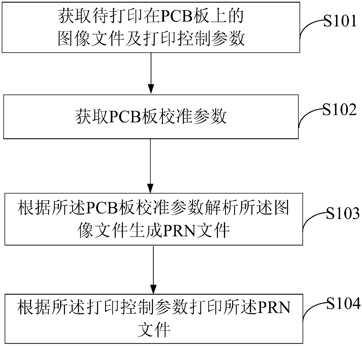
[0051] The first embodiment of the present invention provides a PCB board-oriented printing control method, such as figure 1 As shown, the method includes:

[0052] S101. Acquire an image file to be printed on the PCB and printing control parameters; the image file here may be an image file including a solder mask pattern and / or character pattern to be printed on the PCB;

[0053] Wherein, the image file includes but is not limited to solder resist patterns, character patterns, etc. on the PCB. In this embodiment, the image file is a Gerber file or a preliminary parsed print interface identification file (such as a PRN file). Among them, Gerber file is a two-dimensional vector image file format. It is a standard format used to describe printed circuit board images in printed circuit board industry software. The first step for digital printers to print vector Gerber files is to parse the vector file format into a dot matrix PRN bitmap file format. In this way, the printer can use ...

Embodiment 2

[0089] The second embodiment of the present invention provides a PCB-oriented printing control method, including:

[0090] S201. Obtain an image file to be printed on the PCB and print control parameters;

[0091] S202: Obtain the calibration parameters of the PCB board;

[0092] S203: Analyze the image file according to the PCB board calibration parameters to generate a print interface identification file;

[0093] Among them, steps S201 to S203 are respectively the same as steps S101 to S103 in the first embodiment, and will not be repeated here.

[0094] S204: Print the printing interface identification file according to the printing control parameter.

[0095] Specifically, this step includes:

[0096] S2041. The printing control board receives the printing command with the index of the image to be printed.

[0097] Among them, the printing control board is based on the ARM (English full name: Advanced RISC Machines) platform and runs an embedded Linux system. One end of the print head...

Embodiment 3

[0109] The third embodiment of the present invention provides a PCB board-oriented printing control device, such as Image 6 As shown, the PCB board-oriented printing control device 6 includes:

[0110] The first acquiring module 61 is used to acquire the image file to be printed on the PCB and the printing control parameters;

[0111] The second obtaining module 62 is used to obtain PCB board calibration parameters;

[0112] The parsing module 63 is configured to analyze the image file according to the PCB board calibration parameters to generate a print interface identification file;

[0113] The printing module 64 is configured to print the printing interface identification file according to the printing control parameter.

[0114] The drying control module 65 is used to control the UV lamp to dry the PCB board.

[0115] In a specific implementation, the first obtaining module 41 includes:

[0116] Gerber file acquisition module, used to acquire Gerber files to be printed on the PCB; ...


PUM


Abstract

The invention discloses a PCB (Printed Circuit Board)-oriented printing control method and device, and a storage medium, and relates to the technical field of printing. The method comprises the following steps that: obtaining image files to be printed on the PCB, and printing control parameters; obtaining PCB calibration parameters; according to the PCB calibration parameters, analyzing the imagefiles to generate printing interface identification files; and according to the printing control parameters, printing the printing interface identification files. By use of the method, the image datafile, which is to be printed on the PCB, of a solder resist pattern and a character pattern is obtained, the image data files are calibrated and analyzed into the printing interface identification files which can be identified by an ink-jet printer, and then, the printing interface identification files are input into the ink-jet printer to be analyzed and printed. By use of the method, the solderresist pattern or the character pattern is printed on a PCB substrate in one time, one-time forming can be realized, multi-time repeated printing is not required, and in addition, ink-jet printing ishigh in accuracy and efficiency and has an accurate pattern.

Description

Technical field [0001] The present invention relates to the field of printing technology, and in particular to a printing control method, device and computer-readable storage medium for PCB boards. Background technique [0002] Printed circuit board (PCB, printed circuit board), also known as printed circuit board or printed circuit board, is based on an insulating board, cut into a certain size, and printed some lines, pads / vias, Solder mask, characters and some conductive patterns to realize the interconnection between electronic components. [0003] In the current PCB printing process, it is necessary to coat ink on a substrate made of insulating material, and then dry the ink on the substrate, and then cover the circuit pattern, solder mask pattern, character pattern, etc. to be produced on the coating Expose the ink on the substrate, and finally develop the exposed substrate to complete the circuit printing on the PCB. [0004] The existing production of PCB boards requires ma...

Claims


Application Information

Patent Timeline
IPC IPC(8): H05K3/12B41J29/393
CPCB41J2/01B41J3/407B41J29/38
Inventor 黄振金左国云陈艳
Owner SHENZHEN HOSONSOFT CO LTD