3D ink-jet printer for printing electronic circuit board through ultrasonic atomization nanometer suspending liquid

A nano-suspension and electronic circuit board technology, which is applied in the field of semiconductor functional devices and 3D components, can solve the problem that the printing accuracy of ordinary inkjet printers is difficult to meet the requirements of industrial products, the flow and viscosity of liquids cannot be controlled online, and electronic products are not easy to realize and other issues, to achieve the effect of reducing production time, safe and convenient man-machine operation, and reducing environmental damage

Inactive Publication Date: 2014-09-03
张远明
View PDF8 Cites 25 Cited by
  • Summary
  • Abstract
  • Description
  • Claims
  • Application Information

AI Technical Summary

Problems solved by technology

[0004] Recently, some scholars have put forward the idea of ​​whether ordinary inkjet printers can be used to complete the direct printing of electronic circuit boards, but it can be noted that for the printing of fine lines, it is difficult for ordinary inkjet printers to meet the requirements of industrial products in terms of printing accuracy.
Since the gap between the print nozzle and the printed product of an ordinary inkjet printer is very small, it is not easy to realize electronic products with a three-dimensional structure.
Since the nano-suspension is different from the ink of ordinary inkjet printers, if ordinary inkjet printers are used, it is easy to block the nozzles, and at the same time, it is impossible to control important indicators such as the flow rate and viscosity of the liquid online. And drying also brings great inconvenience

Method used


Image

  • 3D ink-jet printer for printing electronic circuit board through ultrasonic atomization nanometer suspending liquid
  • 3D ink-jet printer for printing electronic circuit board through ultrasonic atomization nanometer suspending liquid
  • 3D ink-jet printer for printing electronic circuit board through ultrasonic atomization nanometer suspending liquid

Examples


Embodiment Construction

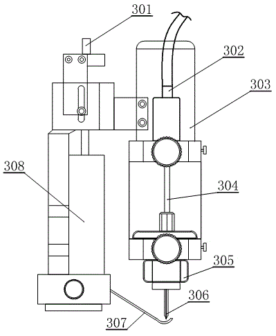
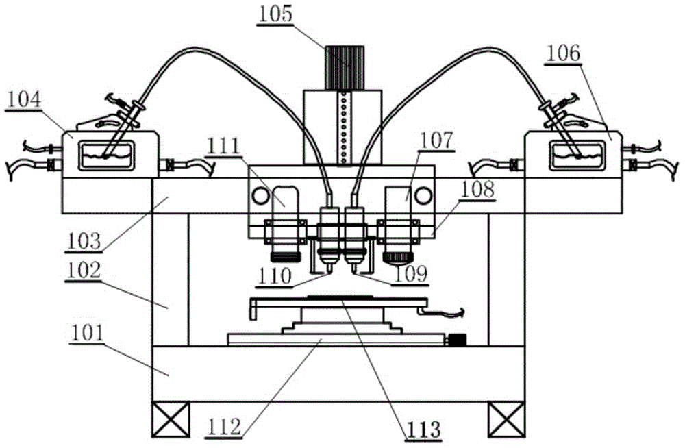
[0029] The invention provides an electronic circuit board 3D inkjet printer based on ultrasonic atomized nano suspension. exist figure 1 Among them, the printer includes a stable marble gantry frame composed of a marble base 101 , a marble column 102 and a marble beam 103 . A high-precision servo-driven XY cross slide 112 is fixed on the marble base 101, and a product table 113 is equipped on it, which can perform XY-axis interpolation motion. A Z-axis servo-driven sliding table 105 is installed on the marble column 102. This sliding table is equipped with a Z-axis sliding block and a fixture 108 for assembling an industrial camera positioner 111, a left nanosuspension printing device 110, and a right The nano-suspension printing device 109 and the infrared laser 107 can complete the functions of positioning, printing and laser sintering. The two sides of the marble frame are respectively equipped with a left ultrasonic nano-suspension atomization device 104 and a right ultr...


PUM

PropertyMeasurementUnit
diameteraaaaaaaaaa

Abstract

The invention discloses a 3D ink-jet printer for printing an electronic circuit board through ultrasonic atomization nanometer suspending liquid. The 3D ink-jet printer comprises an ultrasonic atomization nanometer suspending liquid device, a nanometer fine ink-jet printing device, an industrial positioning camera, a video monitor, an infrared laser micro-fusion-covering device, a heatable vacuum absorption workbench, a three-coordinate movable sliding table and a control portion. According to the 3D ink-jet printer, the nanometer suspending liquid to be printed is atomized based on an ultrasonic double-cavity atomization method, the nanometer suspending liquid is sent to a controllable nanometer fine ink-jet printing device through a guide pipe under the action of auxiliary gas and is directly printed on a substrate in a non-contact mode through a fine ceramic nozzle, the printed nanometer sizing agent is solidified and dried through the method of bottom plate heating or infrared laser micro fusion covering, evaporation of the solvent in the sizing agent, gasification of an organic clad layer and fusion of nanometer particles are accelerated, and therefore the electronic circuit board with high conductivity and micron-size line width is formed. The 3D ink-jet printer can directly print a conducting layer, an insulating layer, a protective layer and a solder mask and can print semiconductor components and parts.

Description

technical field [0001] The invention relates to the field of 3D inkjet printing of electronic circuit boards with atomized nano-suspension, and is especially suitable for directly printing tiny semiconductor functional devices and 3D components. Background technique [0002] In the traditional PCB electronic circuit board manufacturing industry, whether it is ordinary rigid electronic circuit boards or the production of flexible electronic circuit boards in recent years, it must be finally made through a series of complicated processes. Common processes include copper clad laminates. Image, immersion copper, circuit, electroplating, etching, solder mask, text and surface treatment, etc. This production method, on the one hand, requires a relatively large investment in production equipment, which is very inconvenient for small batch production or personalized production, especially the industrial waste gas and waste water generated by the electroplating and etching processes ...

Claims


Application Information

Patent Timeline
Patent Type & Authority Applications(China)
IPC IPC(8): B22F3/105
Inventor 张远明李豹黄淋芳张雨霞
Owner 张远明
Why Eureka
Try Eureka