Lithographic apparatus and device manufacturing method
What is AI technical title?
AI technical title is built by PatSnap AI team. It summarizes the technical point description of the patent document.
a technology of lithographic apparatus and manufacturing method, which is applied in the direction of electrical apparatus, printers, instruments, etc., can solve the problems of unfavorable and unpredictable effects, and achieve the effect of reducing lithography errors
Active Publication Date: 2006-02-16
ASML NETHERLANDS BV
View PDF49 Cites 144 Cited by
Summary
Abstract
Description
Claims
Application Information
AI Technical Summary
This helps you quickly interpret patents by identifying the three key elements:
Problems solved by technology
Method used
Benefits of technology
Benefits of technology
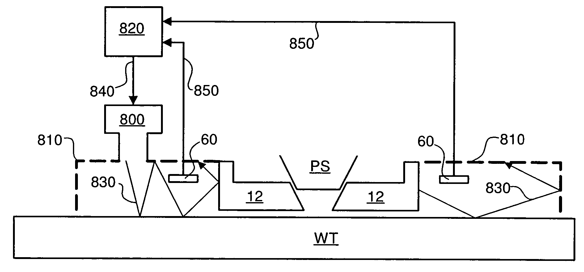
[0009] It is desirable to provide a system that reduces lithography errors arising from the immersion liquid.
Problems solved by technology
This requires additional or more powerful motors and turbulence in the liquid may lead to undesirable and unpredictable effects.
Method used
Image
Click on the blue label to locate the original text in one second.
Reading with bidirectional positioning of images and text.
Examples
Embodiment Construction
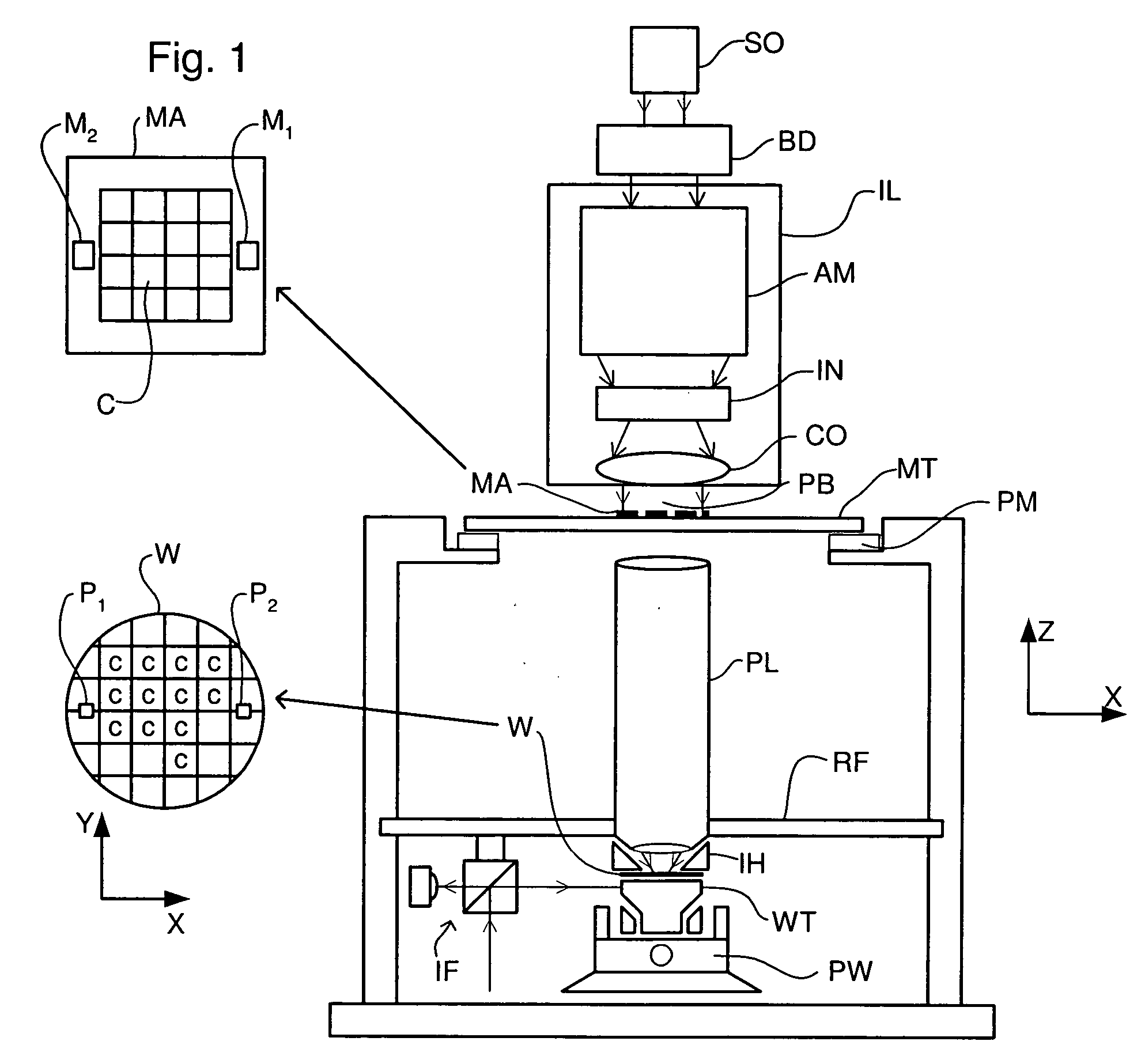
[0043]FIG. 1 schematically depicts a lithographic apparatus according to one embodiment of the invention. The apparatus comprises: [0044] an illumination system (illuminator) IL configured to condition a radiation beam PB (e.g. UV radiation or DUV radiation). [0045] a support structure (e.g. a mask table) MT constructed to support a patterning device (e.g. a mask) MA and connected to a first positioner PM configured to accurately position the patterning device in accordance with certain parameters; [0046] a substrate table (e.g. a wafer table) WT constructed to hold a substrate (e.g. a resist-coated wafer) W and connected to a second positioner PW configured to accurately position the substrate in accordance with certain parameters; and [0047] a projection system (e.g. a refractive projection lens system) PL configured to project a pattern imparted to the radiation beam PB by patterning device MA onto a target portion C (e.g. comprising one or more dies) of the substrate W.
[0048] T...
PUM
Abstract
A lithographic apparatus is disclosed having a liquid supply system configured to at least partly fill a space between a projection system of the lithographic apparatus and a substrate with liquid, a barrier member arranged to substantially contain the liquid within the space, and one or more elements to control and / or compensate for evaporation of liquid from the substrate.
Description
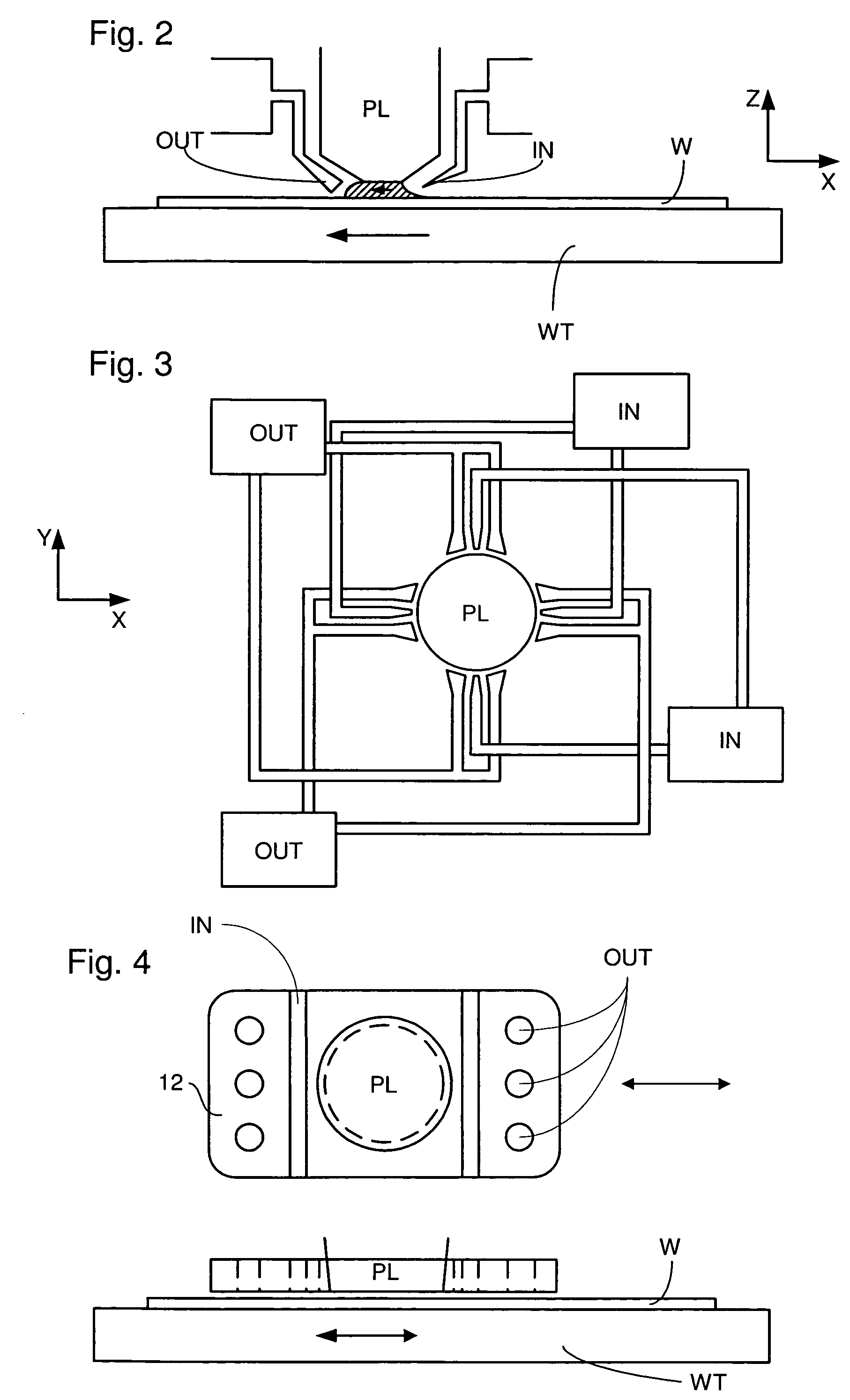
RELATED APPLICATIONS [0001] This application is a continuation-in-part of pending U.S. patent application Ser. No. 10 / 917,535, filed Aug. 13, 2004, the entire contents of which is hereby incorporated by reference.FIELD [0002] The present invention relates to a lithographic apparatus and a method for manufacturing a device. BACKGROUND [0003] A lithographic apparatus is a machine that applies a desired pattern onto a substrate, usually onto a target portion of the substrate. A lithographic apparatus can be used, for example, in the manufacture of integrated circuits (ICs). In that instance, a patterning device, which is alternatively referred to as a mask or a reticle, may be used to generate a circuit pattern to be formed on an individual layer of the IC. This pattern can be transferred onto a target portion (e.g. comprising part of, one, or several dies) on a substrate (e.g. a siliconwafer). Transfer of the pattern is typically via imaging onto a layer of radiation-sensitive materi...
Claims
Application Information
Patent Timeline
Application Date:The date an application was filed.
Publication Date:The date a patent or application was officially published.
First Publication Date:The earliest publication date of a patent with the same application number.
Issue Date:Publication date of the patent grant document.
PCT Entry Date:The Entry date of PCT National Phase.
Estimated Expiry Date:The statutory expiry date of a patent right according to the Patent Law, and it is the longest term of protection that the patent right can achieve without the termination of the patent right due to other reasons(Term extension factor has been taken into account ).
Invalid Date:Actual expiry date is based on effective date or publication date of legal transaction data of invalid patent.
InventorCADEE, THEODORUS PETRUS MARIAJACOBS, JOHANNES HENRICUS WILHELMUSKATE, NICOLAAS TENLOOPSTRA, ERIK ROELOFVERMEER, ASCHWIN LODEWIJK HENDRICUS JOHANNEMARIA MERTENS, JEROEN JOHANNES SOPHIADE MOL, CHRISTIANUS GERARDUS MARIAHUBERTUS MUITJENS, MARCEL JOHANNUS ELISABETHVAN DER NET, ANTONIUS JOHANNUSOTTENS, JOOST JEROENQUAEDACKERS, JOHANNES ANNAREUHMAN-HUISKEN, MARIA ELISABETHSTAVENGA, MARCO KOERTTINNEMANS, PATRICIUS ALOYSIUS JACOBUSVERHAGEN, MARTINUS CORNELIS MARIAHENDRICUS VERSPAY, JACOBUS JOHANNUS LEONARDUSDE JONG, FREDERIK EDUARDGOORMAN, KOENMENCHTCHIKOV, BORISBOOM, HERMANNIHTIANOV, STOYANMOERMAN, RICHARDSMEETS, MARTIN FRANS PIERRESCHOONDERMARK, BART LEONARD PETERJANSSEN, FRANCISCUS JOHANNES JOSEPHRIEPEN, MICHEL

