Bluetooth earphone and power on/off control method thereof
A technology of bluetooth headset and main control circuit, which is applied in the direction of headset mechanical/electronic switch, earpiece/headphone accessories, transducer circuit, etc., which can solve the need for real-time monitoring of voltage on the chip, limited placement of Hall elements, and increased computing load on the chip and other issues, to achieve the effect of low production cost, high signal transmission efficiency, and small chip calculation
- Summary
- Abstract
- Description
- Claims
- Application Information
AI Technical Summary
Problems solved by technology
Method used
Image
Examples
Embodiment 1
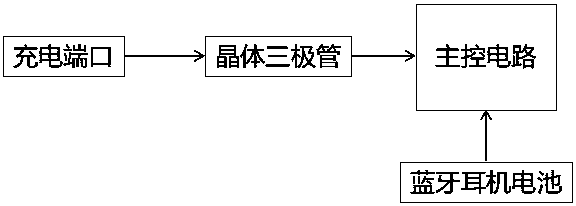
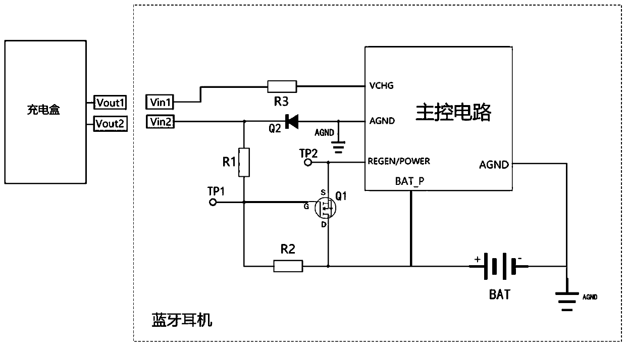
[0039] Embodiment one, including the attached figure 2 The high-level input terminal Vin1, low-level input terminal Vin2, NMOS field effect transistor Q1, first resistor R1, second resistor R2, Bluetooth headset battery BAT and main control circuit shown in the figure. The main control circuit includes a main control chip, and in this embodiment, the model of the main control chip is AB1524_5X5_64L. The first pin of the main control chip is a REGEN / POWER pin, and the second pin is a VCHG pin.
[0040] The high-level input terminal Vin1 is directly connected to the VCHG pin of the main control chip, and the low-level input terminal Vin2 is electrically connected to one end of the first resistor R1. The gate G of the NMOS field effect transistor Q1 is electrically connected to the other end of the first resistor R1 and one end of the second resistor R2 at the same time, and the drain D of the NMOS field effect transistor Q1 is electrically connected to the other end of the sec...
Embodiment 2
[0042] Embodiment two, as attached figure 2 As shown, on the basis of the first embodiment, a diode Q2 is added. The cathode of the diode Q2 is electrically connected to the low-level input terminal Vin2 and one end of the first resistor R1 at the same time, and the anode of the diode Q2 is grounded to the AGND pin of the main control chip.
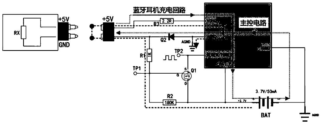
[0043] Embodiment 2 In addition to achieving the technical effect of Embodiment 1, the added diode Q2 can form a charging circuit for the battery of the Bluetooth headset on the one hand, and on the other hand, the diode Q2 connects the first resistor R1, the second resistor R2 and the NMOS The field effect transistor Q1 is isolated from the AGND pin of the main control chip, so that the switch control circuit mainly composed of NMOS field effect transistor Q1, first resistor R1 and second resistor R2 can independently control the Bluetooth headset switch, and at the same time Does not affect the normal operation of the charging circuit...
Embodiment 3
[0044] Embodiment three, as attached figure 2 As shown, on the basis of the second embodiment, the third resistor R3 is added. The high-level input terminal Vin1 is connected to the VCHG pin of the main control chip through the third resistor R3.
PUM
 Abstract
Description
Claims
Application Information
 - R&D
- Intellectual Property
- Life Sciences
- Materials
- Tech Scout
- Unparalleled Data Quality
- Higher Quality Content
- 60% Fewer Hallucinations
Browse by: Latest US Patents, China's latest patents, Technical Efficacy Thesaurus, Application Domain, Technology Topic, Popular Technical Reports.
© 2025 PatSnap. All rights reserved.Legal|Privacy policy|Modern Slavery Act Transparency Statement|Sitemap|About US| Contact US: help@patsnap.com


