A kind of integrated circuit board and preparation method thereof

A technology for integrated circuit boards and substrates, applied in printed circuit manufacturing, printed circuits, electrical components, etc., can solve problems affecting product yield, uneven distribution of resistance of electroplating layers, etc., to reduce losses, reduce contact resistance, improve The effect of forming uniformity

Active Publication Date: 2021-01-22
江门市江海区科诺微电子有限公司
View PDF3 Cites 0 Cited by
  • Summary
  • Abstract
  • Description
  • Claims
  • Application Information

AI Technical Summary

Problems solved by technology

In the prior art, burrs are unavoidable in the production of through holes. Although the number of burrs can be reduced by means of grinding, it still leads to the problem of uneven resistance distribution in the electroplating layer, which directly affects the yield of products.

Method used


Image

  • A kind of integrated circuit board and preparation method thereof
  • A kind of integrated circuit board and preparation method thereof

Examples


specific Embodiment approach

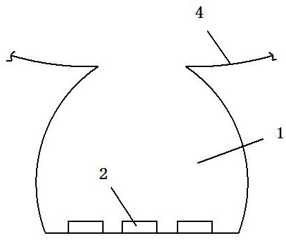
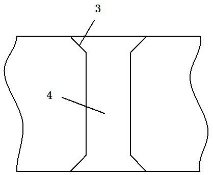
[0031] refer to figure 1 , a specific embodiment of the present invention comprises the following steps:

[0032] A. Perform pretreatment on the substrate, including cleaning and etching;

[0033] B. Perform positioning drilling on the substrate that has been pre-treated in step A, and make through holes 4;

[0034] C. Coating an isolation layer on the inner surface of the through hole 4, and then uniformly opening several grooves 1 along the axial direction on the inner surface of the through hole 4;

[0035] D. Carry out the first electroplating treatment to the groove 1 processed in step C;

[0036] E. Remove the remaining isolation layer on the inner surface of the through hole 4, and then perform a second electroplating treatment on the inner surface of the through hole 4;

[0037] F. Carry out secondary etching after cutting and laminating the substrate;

[0038] G. Coating a solder resist layer on the substrate, and then obtaining a finished integrated circuit board...


PUM


Abstract

The invention discloses a preparation method of an integrated circuit board. The preparation method comprises the following steps of A, performing pretreatment on a substrate, wherein the pretreatmentcomprises cleaning and etching; B, carrying out positioning drilling on the substrate pretreated in the step A, and forming a through hole; C, coating the inner surface of the through hole with an isolation layer, and then uniformly forming a plurality of grooves in the inner surface of the through hole in an axial direction; D, carrying out first electroplating treatment on the grooves formed inthe step C; E, removing the residual isolation layer on the inner surface of the through hole, and then performing second electroplating treatment on the inner surface of the through hole, wherein the isolation layer adopts a wax agent protection layer; F, carrying out board cutting and film pressing on the substrate, and then carrying out secondary etching; and G, coating the substrate with a solder resist layer, and then carrying out surface treatment to obtain the finished integrated circuit board. According to the method, the deficiencies in the prior art can be improved, and the resistance distribution uniformity of a through hole electroplating layer is improved.

Description

technical field [0001] The invention relates to the technical field of integrated circuits, in particular to an integrated circuit board and a preparation method thereof. Background technique [0002] The integrated circuit board is a highly integrated electrical component formed by setting a multi-layer conductive plate and making a corresponding circuit according to the design requirements on the conductive plate. In the integrated circuit board, the current conduction between the conductive plates of different layers should be realized by setting through holes. In the prior art, burrs are unavoidable in the production of through holes. Although the number of burrs can be reduced by means of grinding, it still leads to the problem of uneven resistance distribution in the electroplating layer, which directly affects the yield of products. . Contents of the invention [0003] The technical problem to be solved by the present invention is to provide an integrated circuit ...

Claims


Application Information

Patent Timeline
Patent Type & Authority Patents(China)
IPC IPC(8): H05K3/40
CPCH05K3/4038
Inventor 张超
Owner 江门市江海区科诺微电子有限公司
Why Eureka
Try Eureka