Supercharge Your Innovation With Domain-Expert AI Agents!

Shock wave focus excitation device loading high temperature environment and working method thereof

A shock wave focusing and excitation device technology, which is applied in the direction of microstructure devices, optical waveguide coupling, TV system components, etc., can solve problems such as uneven temperature field distribution and reduced accuracy, and achieve improved reliability and stability performance, improve accuracy, and expand the scope of application

Inactive Publication Date: 2019-04-16
DALIAN UNIV OF TECH
View PDF6 Cites 0 Cited by
  • Summary
  • Abstract
  • Description
  • Claims
  • Application Information

AI Technical Summary

Problems solved by technology

When the above-mentioned heat conduction heating method is used to heat the microstructure, since the heat energy is transferred to the microstructure through the microstructure substrate, the temperature field distribution on the microstructure is very uneven, and the temperature on the microstructure far away from the substrate To be lower than the temperature at the proximal end of the substrate, according to the research results of F, Shen et al. in "Thermal effects on coated resonant microcantilevers", when the temperature field distribution on the microstructure is not uniform, test the dynamic characteristics of the microstructure in a high temperature environment The accuracy of the parameters will be greatly reduced
Therefore, the way of using heat conduction to heat the microstructure in the prior art has great disadvantages

Method used


Image

  • Shock wave focus excitation device loading high temperature environment and working method thereof
  • Shock wave focus excitation device loading high temperature environment and working method thereof
  • Shock wave focus excitation device loading high temperature environment and working method thereof

Examples


Embodiment Construction

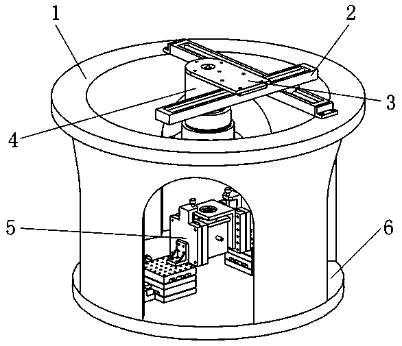
[0028] Figure 1-10 A structural diagram of a shock focusing excitation device loaded with a high temperature environment is shown.

[0029] figure 1 Among them, the shock wave focusing excitation device loaded in a high-temperature environment includes a cylinder body 1, a motorized two-axis translation stage 2, a mounting plate 3, an optical heating unit 4, and a microstructure excitation unit 5. The bottom plate 6 of the cylinder 1 is provided with a microstructure excitation unit 5 , and the top of the cylinder 1 is provided with an electric two-axis translation platform 2 , and an optical heating unit 4 is installed on the slider of the electric two-axis translation platform 2 through a mounting plate 3 .

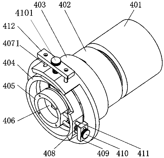
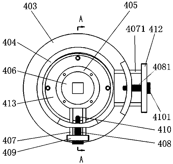
[0030] figure 2 , 3 Among them, the optical heating unit 4 includes a front sleeve 403 , a connecting sleeve 402 and a rear sleeve 401 which are screwed in sequence, and a parallel light source 415 is arranged in the central hole at the tail of the rear sleeve 401 . ...


PUM


Abstract

The invention relates to a shock wave focus excitation device loading a high temperature environment and a working method thereof, belonging to the technical field of micro-electro-mechanical systems.The device comprises a cylinder, an electric driven two-shaft displacement table, a light heating unit, and a micro-structure excitation unit, wherein the micro-structure excitation unit is providedwith a shock wave focus cavity at a bottom center of a second connection plate, a semi-ellipsoidal cavity is arranged on the upper end surface of the shock wave focus cavity, needle electrodes are respectively sheathed on two opposite side surfaces of the shock wave focus cavity through ceramic tubes, the tip of each needle electrode is nearby the focus in the semi-ellipsoidal cavity, and a distance between tips of the two needle electrodes is 0.5-1.0mm. The light heating unit adopts a shading sheet and a shading plate, so that parallel light emitted by the light heating unit radiates an MEMSmicro-structure alone. The device can heat the overall MEMS micro-structure, guarantees uniform temperature distribution on the micro-structure surface, lowers temperature gradient on the micro-structure surface, and makes tests of micro-structure dynamic characteristic parameters in high temperature much more accurate.

Description

technical field [0001] The invention relates to a shock wave focusing excitation device loaded in a high-temperature environment and a working method thereof, belonging to the technical field of micromechanical electronics. Background technique [0002] Due to the characteristics of low cost, small size, light weight, high integration and high degree of intelligence, MEMS micro devices have been widely used in automobiles, aerospace, information communication, biochemistry, medical treatment, automatic control, consumer goods and national defense. fields have been widely applied. When designing and developing MEMS, because the system function is mainly realized by the micro-displacement and deformation of the microstructure, it is necessary to measure the dynamic performance of the micro-mechanical components, so the mechanical motion parameters of MEMS such as displacement, velocity, amplitude, frequency and vibration mode Accurate measurement has become an important part ...

Claims


Application Information

Patent Timeline
Patent Type & Authority Applications(China)
IPC IPC(8): B81B7/02
CPCB81B7/02
Inventor 田江平崔靖晨田华隆武强冯立岩武文华
Owner DALIAN UNIV OF TECH
Features
  • R&D
  • Intellectual Property
  • Life Sciences
  • Materials
  • Tech Scout
  • Unparalleled Data Quality
  • Higher Quality Content
  • 60% Fewer Hallucinations
Learn More