

Method of controlling mass transfer of Micro-LEDs by using ultrasonic standing waves
An ultrasonic standing wave and ultrasonic technology, which is applied in electrical components, circuits, semiconductor devices, etc., can solve the problems that the distance between the wafers cannot adapt to the target substrate, and the uniformity and consistency of the elastic film are high.
- Summary
- Abstract
- Description
- Claims
- Application Information
AI Technical Summary
Problems solved by technology
Method used
Image

Examples
Embodiment Construction
[0033] The technical solutions of the present invention will be further described below in conjunction with the accompanying drawings and through specific implementation methods.
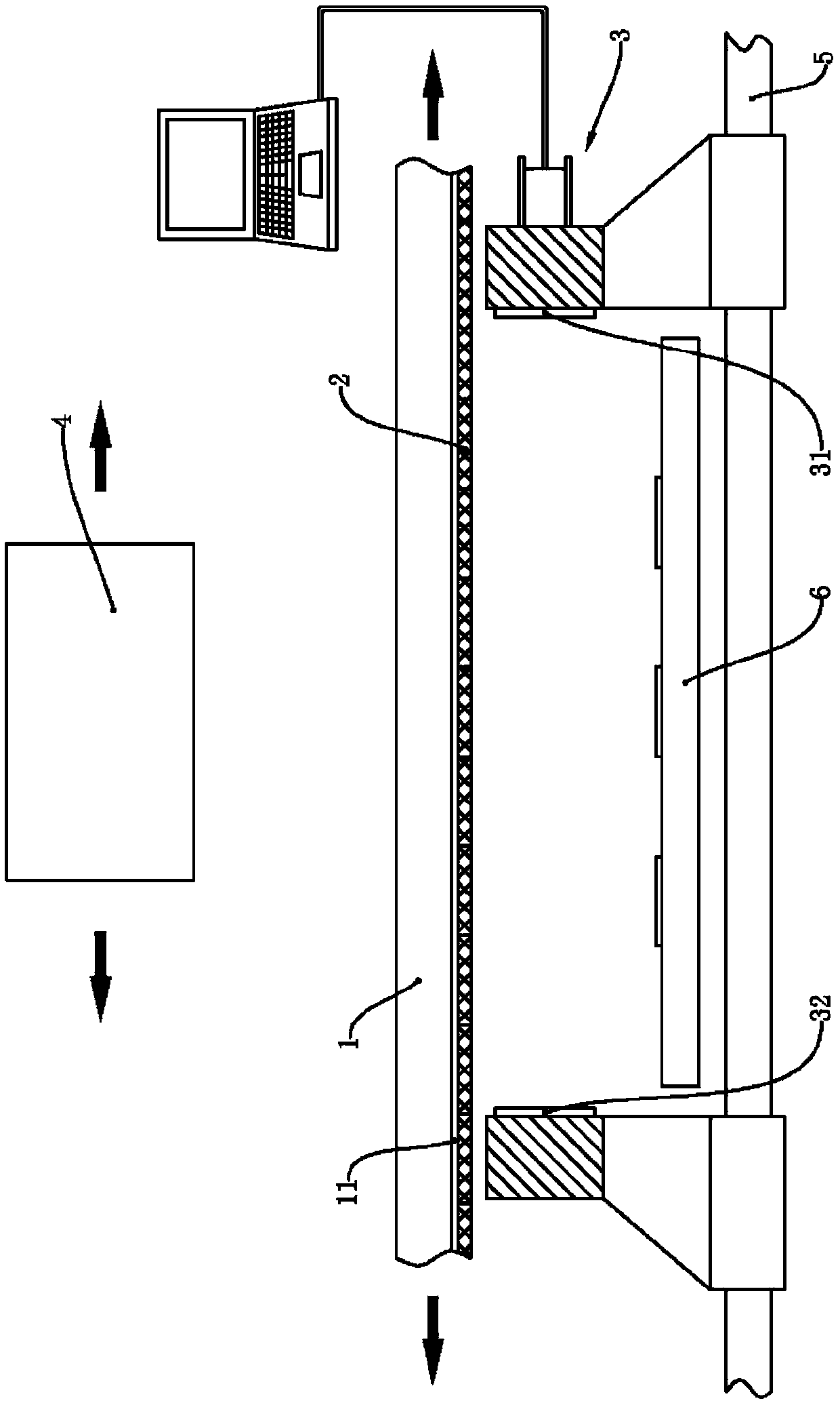
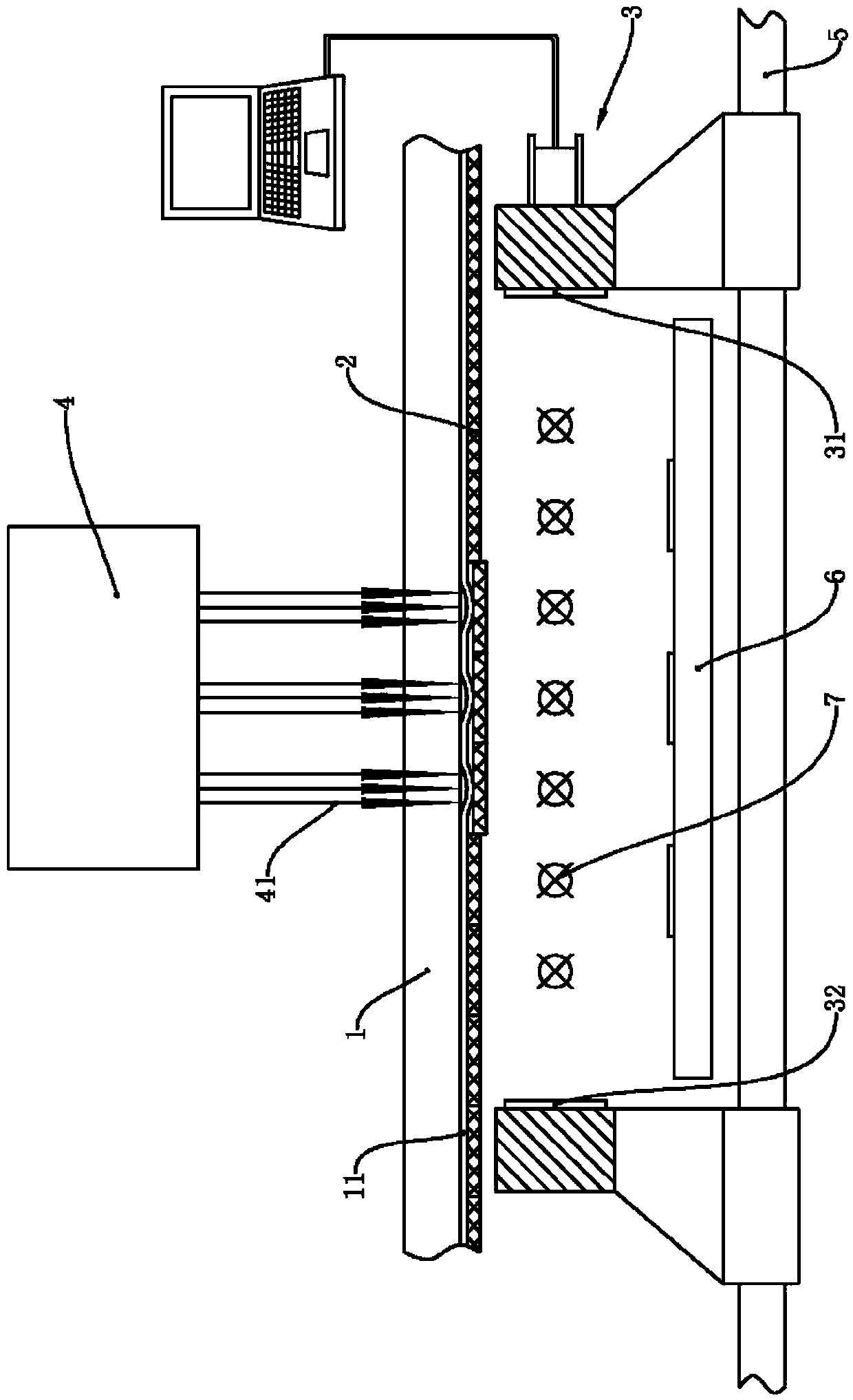
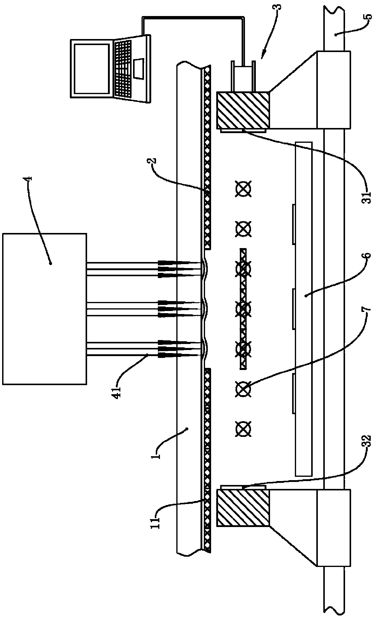
[0034] A method of manipulating the mass transfer of Micro-LEDs using ultrasonic standing waves in this embodiment, such as Figure 1-5 As shown, it includes: a transfer substrate 1, a Micro-LED chip 2, an ultrasonic transducer 3, a laser emitter 4, a guide rail 5 and a target substrate 6;
[0035] The transfer substrate is provided with an elastic layer 11, and the Micro-LED chip 2 is disposed on the elastic layer 11 of the transfer substrate 1;
[0036] The ultrasonic transducer 3 emits ultrasonic waves, the ultrasonic transducer includes a radiation end surface 31 and a reflection end surface 32, and the ultrasonic transducer 3 generates a sound pressure node 7 between the radiation end surface 31 and the reflection end surface 32;
[0037] The transfer substrate 1 is arranged above the guide ra...
PUM
 Abstract
Description
Claims
Application Information