
Tunable coupled cavity semiconductor laser

A coupled cavity and semiconductor technology, applied in the field of tunable coupled cavity semiconductor lasers, can solve problems such as complex processes, and achieve the effects of simple manufacturing process, overcoming high cost, and reducing loss

Active Publication Date: 2019-04-16
INST OF SEMICONDUCTORS - CHINESE ACAD OF SCI
View PDF8 Cites 0 Cited by
  • Summary
  • Abstract
  • Description
  • Claims
  • Application Information

AI Technical Summary

Problems solved by technology

However, the process of tunable lasers adjusted based on gratings is very complicated due to the need for secondary epitaxy and high-precision gratings in the manufacturing process.

Method used


Image

  • Tunable coupled cavity semiconductor laser
  • Tunable coupled cavity semiconductor laser
  • Tunable coupled cavity semiconductor laser

Examples


Embodiment Construction

[0039]Whispering gallery mode microcavity utilizes the total reflection of light at the interface to form a resonant mode. It has the advantages of small size, low threshold, low power consumption, and easy integration. It is widely used in photonic integrated circuits, optical interconnections, optical communications, and microwave photonics. and other fields. Compared with traditional semiconductor lasers, due to its high quality factor and small size, it has shown obvious advantages in direct high-speed modulation. However, the whispering gallery mode microcavity laser has a smaller cavity volume and lower output power than traditional lasers, so a certain trade-off needs to be made between the output power and the single-mode nature of the cavity. In addition, in the prior art, although the coupling cavity structure formed by conventionally shaped whispering gallery microcavities such as disk, circular, regular polygon or ellipse and FP cavity has significantly improved th...


PUM


Abstract

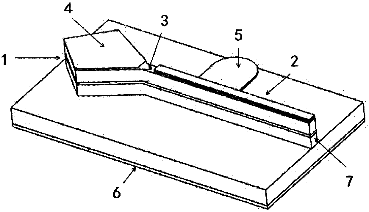
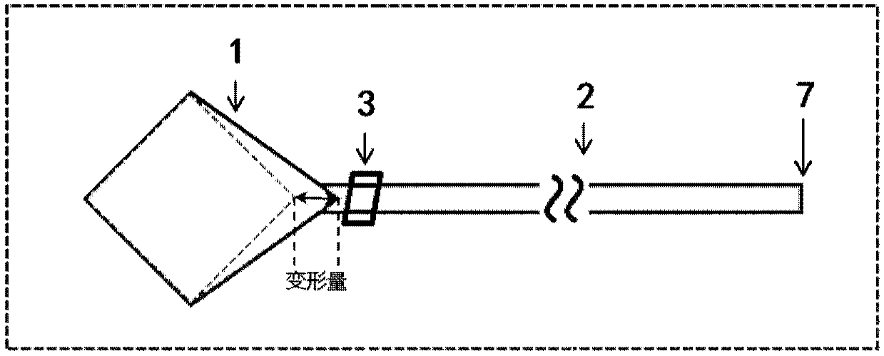
The invention discloses a tunable coupled cavity semiconductor laser, which comprises an FP cavity; a variable echo wall micro-cavity connected with the first end of the FP cavity and served as a reflection end face of the FP cavity, wherein the variable echo wall micro-cavity and the FP cavity form a coupled cavity structure; and an electric isolation groove formed between the FP cavity and the variable echo wall micro-cavity. The light enters the variable echo wall micro-cavity after being incident from the second end of the FP cavity. After that, the light with the specific wavelength is reflected back to the FP cavity after being reflected in the variable echo wall micro-cavity. According to the tunable coupled cavity laser, the fundamental mode proportion of a coupling mode of laser emission of the tunable coupled cavity laser in an FP cavity is very high, so that the loss of light in the FP cavity is reduced. Meanwhile, the laser emission mode of the coupled cavity is more stable, and the output power is higher. At the same time, the equivalent reflectivity spectrum of the deformable echo wall micro-cavity is insensitive to gain change in the cavity, and the laser emission mode is not liable to jump to an adjacent longitudinal mode. As a result, the tunable coupled cavity laser can obtain a large wavelength tuning range.

Description

technical field [0001] The disclosure belongs to the technical fields of optical fiber communication and semiconductor lasers, and relates to a tunable coupling cavity semiconductor laser. Background technique [0002] Wavelength tunable lasers are an important part of wavelength division multiplexing systems, and also one of the key components of photonic integrated circuits and next-generation reconfigurable optical networks. With the rapid development of optical communication technology, tunable semiconductor lasers are constantly moving towards low cost, low power consumption, high side mode suppression ratio, high output power, high wavelength switching speed, narrow linewidth and monolithic integration, and high direction of modulation rate. Starting from practical applications, it is required that tunable lasers can be tuned in a wide range, low in cost, stable in operation and easy to operate. [0003] Currently, commercially available monolithically integrated wid...

Claims


Application Information

Patent Timeline
Patent Type & Authority Applications(China)
IPC IPC(8): H01S5/10
CPCH01S5/1021H01S5/1039H01S5/1042
Inventor 郝友增黄永箴杨跃德肖金龙王福丽汤敏翁海中
Owner INST OF SEMICONDUCTORS - CHINESE ACAD OF SCI
Learn More