Wafer film covering device

A technology for laminating devices and wafers, which is applied in the manufacturing of electrical components, electric solid-state devices, semiconductor/solid-state devices, etc., and can solve the problems of film deformation, wrinkles, and low efficiency.

Active Publication Date: 2019-04-19
ANHUI LONGXINWEI TECH CO LTD
View PDF3 Cites 3 Cited by
  • Summary
  • Abstract
  • Description
  • Claims
  • Application Information

AI Technical Summary

Problems solved by technology

[0007] The present invention intends to provide a wafer coating device to solve the problem that in the prior art, when the film is cut, the peripheral film will be d...

Method used


Image

  • Wafer film covering device
  • Wafer film covering device
  • Wafer film covering device

Examples


Embodiment Construction

[0020] The following is further described in detail through specific implementation methods:

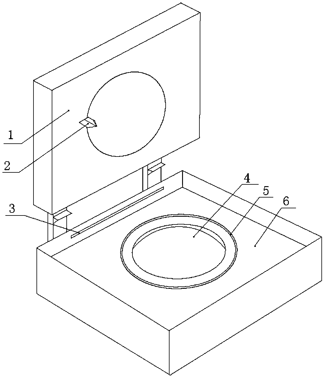
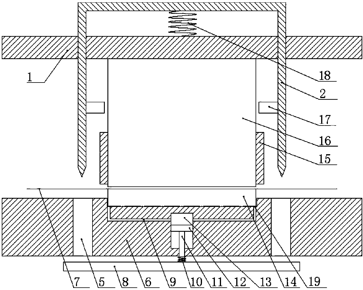
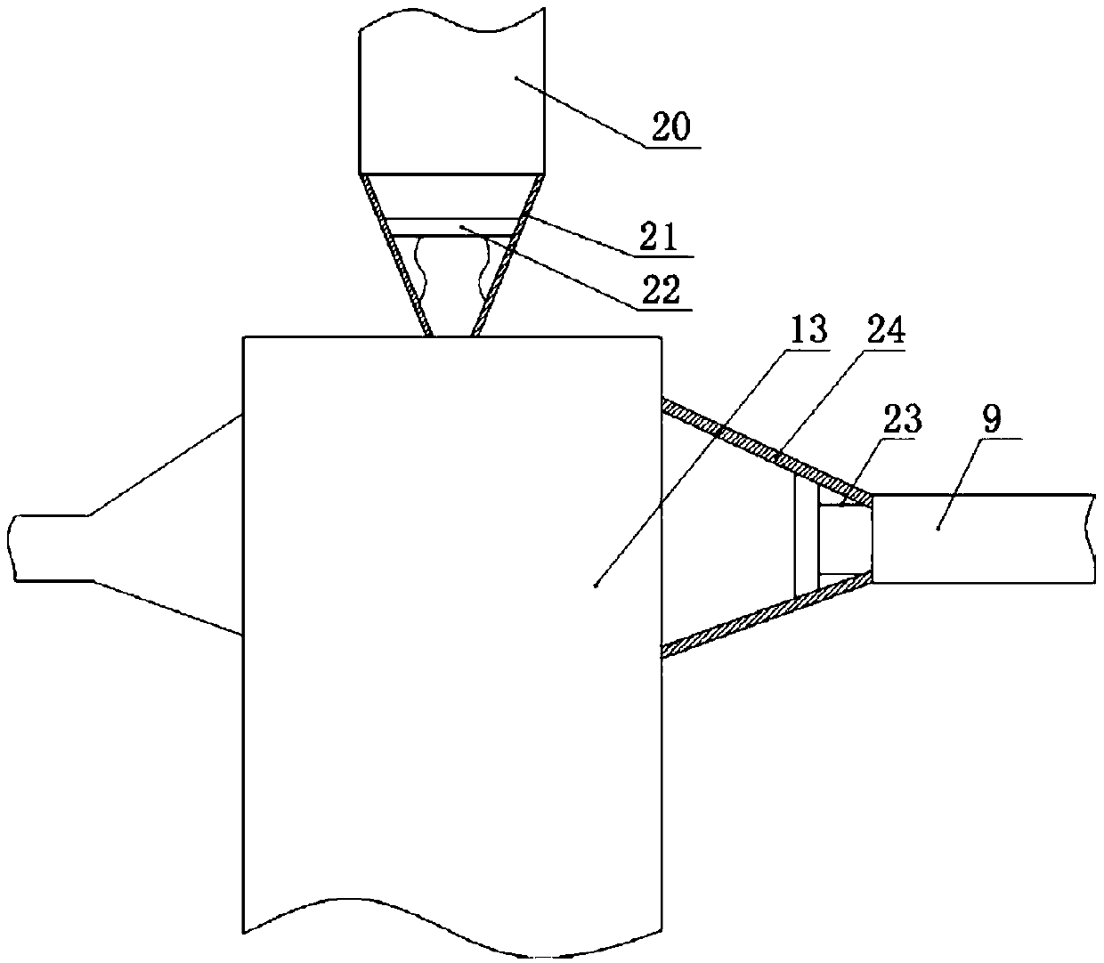
[0021] The reference signs in the drawings of the description include: cover body 1, cutter 2, feeding hole 3, placement groove 4, cutting hole 5, bottom box 6, film 7, bottom plate 8, suction channel 9, negative pressure spring 10, Piston rod 11, piston 12, negative pressure chamber 13, wafer 14, hemming cylinder 15, pressure column 16, push plate 17, cutting spring 18, suction hole 19, air outlet pipe 20, air outlet connecting pipe 21, sealing plate 22 , elastic cord 23, air intake connecting pipe 24.

[0022] Such as figure 1 As shown, the laminating machine in the prior art includes a bottom box 6, and the side wall of the bottom box 6 is provided with a feed hole 3, and the bottom box 6 is provided with a placement groove 4 for placing a wafer 14, and the placement groove 4 is concentric with it An annular cutting hole 5 is provided, and a cover body 1 is hinged on one side of...


PUM


Abstract

The invention relates to the technical field of electric appliance element manufacturing, and specifically relates to a wafer film covering device. The device comprises a bottom box, a feeding hole isformed in a side wall of the bottom box. The bottom box is provided with a placing groove used for placing a wafer. An annular cutting hole is formed outside the containing groove and concentric withthe containing groove, a cover body is hinged to one side of the bottom box, a cylindrical cutter is vertically arranged on the cover body in a sliding mode, the cutter can drive the edge covering mechanism, a cutting spring is arranged between the cutter and the cover body, and a cylindrical pressing column is arranged on the inner side of the cover body. The problems that in the prior art, whena thin film is cut, a peripheral thin film is deformed and wrinkled under the acting force of the rotating direction, and the efficiency is not high due to the fact that the peripheral thin film needs to be manually wrapped on a wafer are solved.

Description

technical field [0001] The invention relates to the technical field of manufacturing electrical components, in particular to a wafer coating device. Background technique [0002] Wafer refers to the silicon wafer used in the production of silicon semiconductor integrated circuits. Because of its circular shape, it is called a wafer. It can be processed into various circuit element structures on silicon wafers, and become IC products with specific electrical functions. [0003] The wafer is drawn and refined from ordinary silica sand, and after a series of measures of dissolution, purification, and distillation, it is made into a single crystal silicon rod. After the single crystal silicon rod is polished and sliced, it becomes a wafer. After the wafer is fabricated, it needs to be covered with a film to protect the wafer and avoid wafer wear. [0004] Traditional wafer cutting is usually manual operation. The film is covered on the wafer, and the worker holds the cutter an...

Claims


Application Information

Patent Timeline
IPC IPC(8): H01L21/683
CPCH01L21/6836H01L2221/68327
Inventor 黄晓波赵凡奎
Owner ANHUI LONGXINWEI TECH CO LTD
Why Eureka
Try Eureka