

Organic electroluminescence device and display device
An electroluminescent device and luminescent technology, which is applied in the direction of electric solid-state devices, electrical components, semiconductor devices, etc., can solve the problems of low luminous efficiency and low life of devices, achieve good transmission performance, improve luminous efficiency and life, and prolong The effect of service life
- Summary
- Abstract
- Description
- Claims
- Application Information
AI Technical Summary
Problems solved by technology
Method used
Image

Examples
Embodiment 1-11
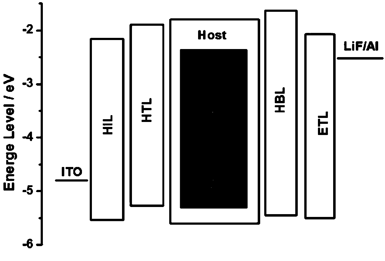
[0062] Such as image 3 As shown, each of Embodiments 1-11 provides an organic electroluminescent device, which successively includes an anode, a hole injection layer (HIL), a hole transport layer (HTL), a light emitting layer (EML), a hole blocking layer (HBL) ), electron transport layer (ETL), electron injection layer (EIL) and cathode.
[0063] The device structure of embodiment 1 is ITO / HATCN (10nm) / NPB (40nm) / main body: 30%T-76:5%F-8 (30nm) / hole blocking (5nm) / TPBI (30nm) / LiF ( 1nm) / Al(200nm).
[0064] The device structure of Examples 2-11 is basically the same as that of Example 1, the only difference lies in the materials and / or doping concentrations of the light emitting layer and the hole blocking layer.
[0065] In the organic electroluminescent devices provided in Examples 1-11, the specific selection and doping concentration of the materials of the light-emitting layer and the hole blocking layer, and the test results of the corresponding organic electroluminesce...
Embodiment 12-15
[0080] Such as image 3 As shown, Examples 12-15 respectively provide an organic electroluminescence device, the device structure is basically the same as that of Example 1, the only difference is that the doping concentration of the sensitizer in the light-emitting layer is different, and the specific concentration of the sensitizer in the light-emitting layer is different. The doping concentration and the test results of the corresponding organic electroluminescent devices are shown in Table 3.
[0081] table 3
[0082]
[0083] From the test results in Table 3 combined with Table 1, it can be seen that as the doping concentration of the TADF material used as a sensitizer in the light-emitting layer changes, the luminous efficiency and service life of the corresponding OLED device also change accordingly. When the doping concentration of the TADF material in the light-emitting layer is 10-40wt%, the OLED device has relatively optimal luminous efficiency and service life....
Embodiment 16-19
[0086] Such as image 3 As shown, Examples 16-19 respectively provide an organic electroluminescence device, the structure of the device is basically the same as that of Example 2, the only difference lies in the thickness of the hole blocking layer. Table 4 shows the thickness of the hole blocking layer and the test results of the corresponding organic electroluminescent devices in specific examples 15-18.
[0087] From Table 4 and in conjunction with the test results of the aforementioned Examples 1-15, it can be known that when the light-emitting layer uses TADF material as the sensitizer, and the hole blocking layer contains TADF material, as the thickness of the hole blocking layer changes, the OLED device Both luminous efficiency and service life have changed. When the thickness of the hole blocking layer is 1-50nm, the luminous efficiency of the OLED device is relatively high and the service life is relatively long, especially when the thickness of the hole blocking la...
PUM
 Abstract
Description
Claims
Application Information