
Microchannel plate and method for preparing high-resistance thin film with Cu being doped with Al2O3 on inner wall of microchannel plate

A technology of microchannel plate and microchannel, which is applied in the field of thin film doping, can solve the problems of resistivity change and unstable performance of microchannel plate, and achieve the effect of compact structure, excellent thermal stability and smooth surface

Inactive Publication Date: 2019-04-26
XI'AN INST OF OPTICS & FINE MECHANICS - CHINESE ACAD OF SCI
View PDF2 Cites 4 Cited by
  • Summary
  • Abstract
  • Description
  • Claims
  • Application Information

AI Technical Summary

Problems solved by technology

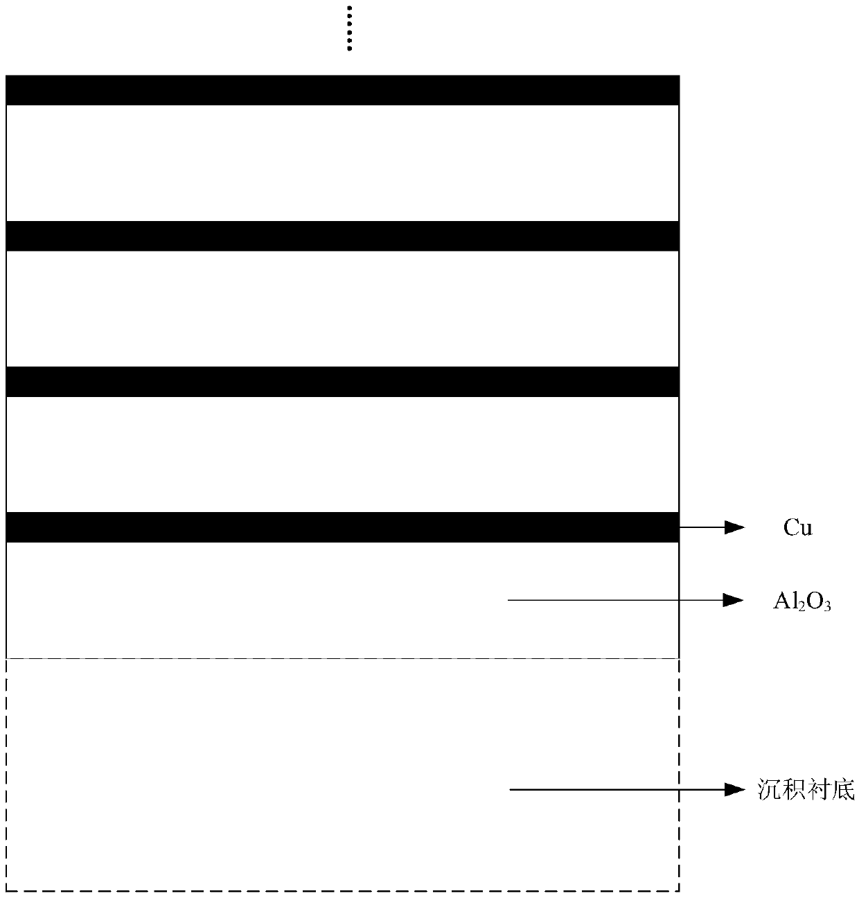
[0004] In order to solve the technical problem that the performance of the microchannel plate is unstable due to the large resistivity change of the surface film of the existing microchannel plate under high temperature conditions, the present invention provides a microchannel plate and the preparation of Cu-doped Al on the inner wall of the microchannel plate 2 o 3 High resistance thin film method

Method used


Image

  • Microchannel plate and method for preparing high-resistance thin film with Cu being doped with Al2O3 on inner wall of microchannel plate
  • Microchannel plate and method for preparing high-resistance thin film with Cu being doped with Al2O3 on inner wall of microchannel plate
  • Microchannel plate and method for preparing high-resistance thin film with Cu being doped with Al2O3 on inner wall of microchannel plate

Examples


Embodiment 1

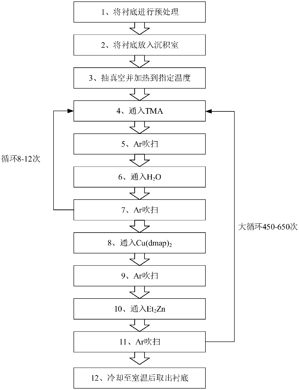
[0046] Place the microchannel plate in RCA standard cleaning solution SC-2 (HCl: H 2 o 2 :H 2 O=1:1:5), after ultrasonic cleaning at 85°C for 10 minutes, placed in HF solution (HF:H 2 (0=1:50) after ultrasonic cleaning, put the microchannel plate into the atomic layer deposition chamber, and vacuumize to 10 -1 Pa, and the temperature of the deposition chamber and the microchannel plate was heated to 100 °C, and the Al 2 o 3 deposition, i.e. TMA / Ar / H 2 O / Ar=(0.03s / 10s / 0.03s / 10s), after 12 cycles, 1 Cu deposition, ie Cu(dmap) 2 / Ar / Et 2 Zn / Ar=(2s / 10s / 0.5s / 10s), 12 times Al 2 o 3 After the deposition cycle and 1 Cu deposition is a large cycle, the deposition is stopped after 450 large cycles, and after the deposition chamber is lowered to room temperature, the deposition chamber is opened, and the deposited Cu-doped Al 2 o 3 Thin film microchannel plate.

Embodiment 2

[0048] Place the microchannel plate in RCA standard cleaning solution SC-2 (HCl: H 2 o 2 :H 2 O=1:1:5), after ultrasonic cleaning at 85°C for 10 minutes, placed in HF solution (HF:H 2 (0=1:50) after ultrasonic cleaning, put the microchannel plate into the atomic layer deposition chamber, and vacuumize to 10 -2 Pa, and the temperature of the deposition chamber and the microchannel plate was heated to 105 °C, and the Al 2 o 3 deposition, i.e. TMA / Ar / H 2 O / Ar=(0.03s / 10s / 0.03s / 10s), after 11 cycles, 1 Cu deposition, ie Cu(dmap) 2 / Ar / Et 2 Zn / Ar=(2s / 10s / 0.5s / 10s), 11 times Al 2 o 3 After the deposition cycle and 1 Cu deposition is a large cycle, the deposition is stopped after 500 large cycles, and after the deposition chamber is lowered to room temperature, the deposition chamber is opened, and the deposited Cu-doped Al 2 o 3 Thin film microchannel plate.

Embodiment 3

[0050] Place the microchannel plate in RCA standard cleaning solution SC-2 (HCl: H 2 o 2 :H 2 O=1:1:5), after ultrasonic cleaning at 85°C for 10 minutes, placed in HF solution (HF:H 2 (0=1:50) after ultrasonic cleaning, put the microchannel plate into the atomic layer deposition chamber, and vacuumize to 10 -3 Pa, and the temperature of the deposition chamber and the microchannel plate was heated to 110°C, and the Al 2 o 3 deposition, i.e. TMA / Ar / H 2 O / Ar=(0.03s / 10s / 0.03s / 10s), after 10 cycles, 1 Cu deposition, ie Cu(dmap) 2 / Ar / Et 2 Zn / Ar=(2s / 10s / 0.5s / 10s), 10 times Al 2 o 3 After the deposition cycle and one Cu deposition is a large cycle, the deposition is stopped after 550 large cycles, and after the deposition chamber is lowered to room temperature, the deposition chamber is opened, and the deposited Cu-doped Al 2 o 3 Thin film microchannel plate.


PUM

PropertyMeasurementUnit
Resistivityaaaaaaaaaa

Abstract

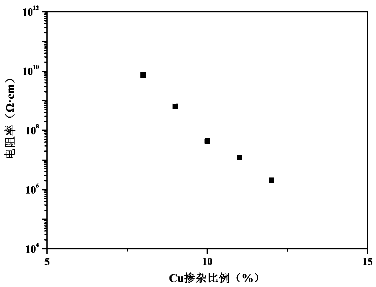
The invention relates to a microchannel plate and a method for preparing a high-resistance thin film with Cu being doped with Al2O3 on the inner wall of the microchannel plate. According to preparation of the high-resistance thin film with the Cu being doped with the Al2O3 on the inner wall of the microchannel plate, the high-resistance thin film with the Cu being doped with the Al2O3 is obtainedby the manner that different composition material deposition is performed on the inner wall of the microchannel plate through an atomic layer deposition method, when the deposition is performed, in one large circulation, the Cu doping ratio is controlled by controlling the deposition times of the Al2O3 and the deposition times of the Cu, so that the resistance rate of the thin film can be accurately adjusted and controlled within the range of 10<6>-10<10> omega.cm, the thickness of the thin film is controlled by controlling the circulation times of the large circulation, the resistance rate ofthe prepared thin film basically remains constant under a high-temperature working environment or after high-temperature annealing, and the technical problem of unstable performance of the microchannel plate caused by large change of the resistance rate of an existing microchannel plate surface thin film under the high-temperature condition is solved.

Description

technical field [0001] The invention belongs to the technical field related to film doping, and relates to a method for preparing a high-resistance film of a photoelectric material, in particular to a method for preparing Cu-doped Al on the inner wall of a microchannel plate. 2 o 3 High resistance film method. Background technique [0002] After the traditional lead-silicate glass microchannel plate has been processed through a complex preparation process, the surface roughness of the inner wall is high, which will lead to problems such as reduced gain and increased noise, which limits further improvement of its performance. The performance of the microchannel plate can be further improved by preparing the functional layer on the inner wall of the microchannel plate through the thin film preparation process. At present, the functional layer of the microchannel plate is prepared separately by the atomic layer deposition (Atomic Layer Deposition) thin film preparation technol...

Claims


Application Information

Patent Timeline
IPC IPC(8): C23C16/455C23C16/40C23C16/18H01J43/24
CPCC23C16/18C23C16/403C23C16/45529H01J43/246
Inventor 郭俊江彭波郭海涛朱香平许彦涛曹伟伟邹永星陆敏
Owner XI'AN INST OF OPTICS & FINE MECHANICS - CHINESE ACAD OF SCI
Learn More