Silicon-based OLED product

A silicon-based and product technology, applied in the field of silicon-based OLED products, can solve the problems of small size and high cost, and achieve the effect of reducing the area and realizing the narrow frame.

Inactive Publication Date: 2019-05-07
SEEYA OPTRONICS LTD
View PDF5 Cites 7 Cited by
  • Summary
  • Abstract
  • Description
  • Claims
  • Application Information

AI Technical Summary

Problems solved by technology

[0004] In existing silicon-based OLED panel display products, there are mainly two positional relationships between the IC that provides various signals and the display panel: 1) The IC is directly integrated on t

Method used


Image

  • Silicon-based OLED product
  • Silicon-based OLED product
  • Silicon-based OLED product

Examples


Embodiment Construction

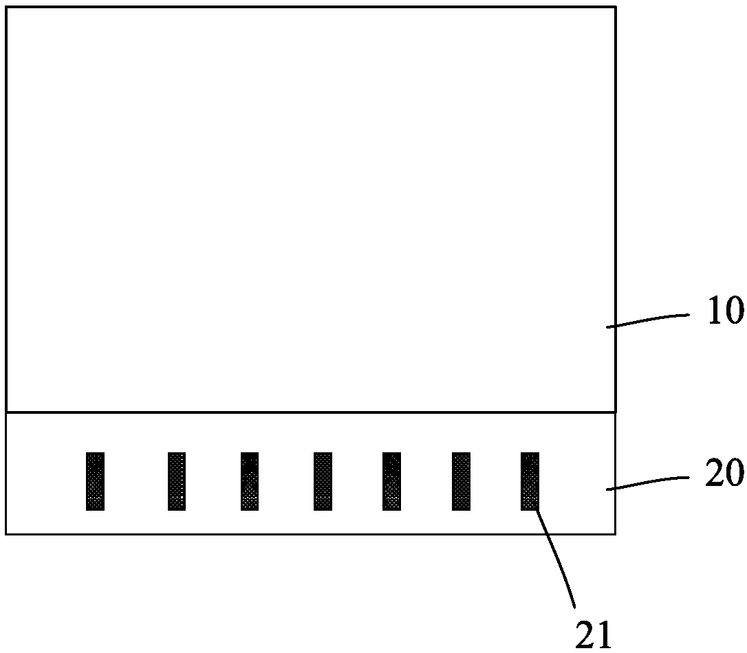
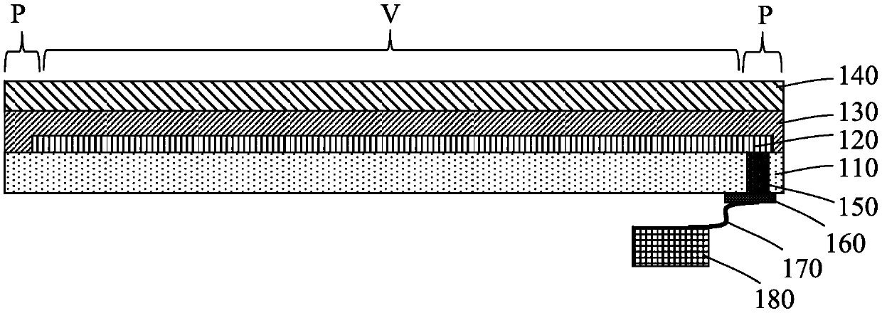
[0024] In silicon-based OLED products, when the chips originally produced outside are integrated into the silicon-based OLED display panel, that is, when the corresponding integrated circuits are integrated in the silicon-based OLED display panel, the corresponding cost will be very high, and it will also occupy Large product area.

[0025] Therefore, one way to reduce the cost is to use externally bonded chips instead of making corresponding integrated circuits in the display panel.

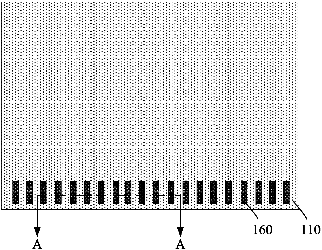
[0026] However, when the corresponding integrated circuit is not produced in the display panel, but chooses to bind external chips, due to the high resolution of the corresponding product, there are too many source signal lines, which leads to too many bonding pads for the chip The problem. Due to the limited size of the silicon-based OLED display panel, it is impossible to manufacture a large number of bonding pads to the edge area of ​​the display panel, so the bonding pads have to be placed ...


PUM


Abstract

A silicon-based OLED product comprises a silicon-based OLED display panel and a chip, the silicon-based OLED display panel is provided with a first surface and a second surface, the first surface is used for facing a user when a picture is displayed, and the second surface is opposite to the first surface; a binding gasket is arranged on the second surface; and the chip is bound with the silicon-based OLED display panel through the binding gasket. The performance of the silicon-based OLED product is improved.

Description

technical field [0001] The invention relates to the field of semiconductor manufacturing, in particular to a silicon-based OLED product. Background technique [0002] Silicon-based OLED display devices are different from conventional AMOLED devices that use amorphous silicon, microcrystalline silicon or low-temperature polysilicon thin-film transistors as backplanes. much higher than conventional devices. [0003] Among them, the monocrystalline silicon chip can adopt the existing mature integrated circuit CMOS technology, which not only realizes the active addressing matrix of the display screen pixels, but also realizes such as SRAM memory and timing controller (timing controller, TCON) on the silicon chip. The drive control circuit with multiple functions greatly reduces the external wiring of the device, increases reliability and realizes light weight. [0004] In existing silicon-based OLED panel display products, there are mainly two positional relationships between ...

Claims


Application Information

Patent Timeline
IPC IPC(8): H01L27/32
Inventor 钱栋李启张萍
Owner SEEYA OPTRONICS LTD
Why Eureka
Try Eureka