Reconfigurable general-purpose metamaterial
A metamaterial, general-purpose technology, applied to electrical components, antennas, etc., can solve the problem of uncontrollable dual negative frequency bands
- Summary
- Abstract
- Description
- Claims
- Application Information
AI Technical Summary
Problems solved by technology
Method used
Image
Examples
Embodiment 1
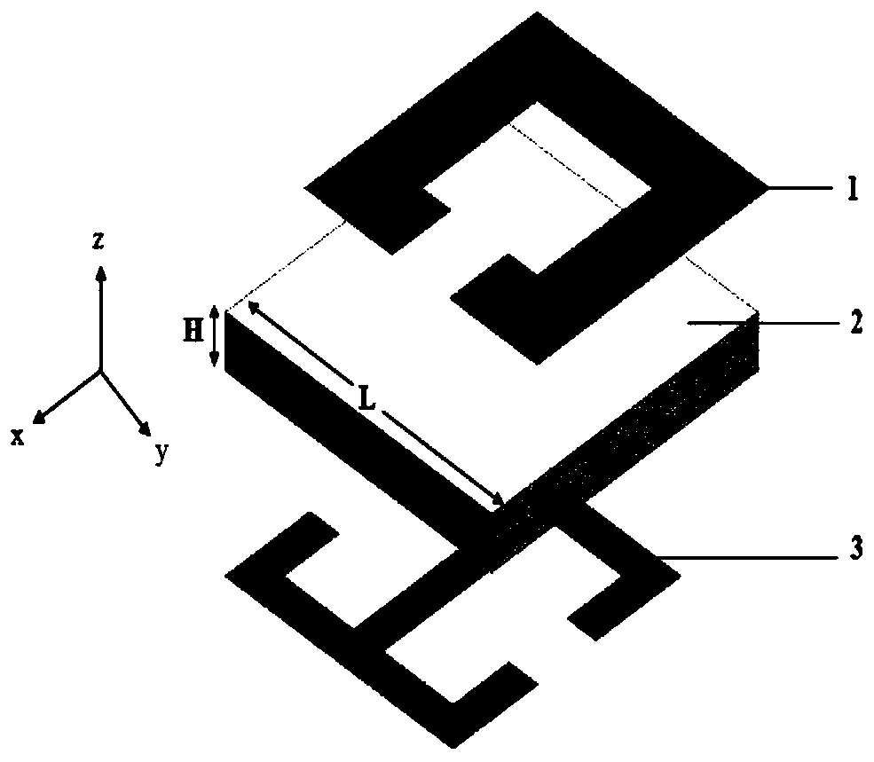
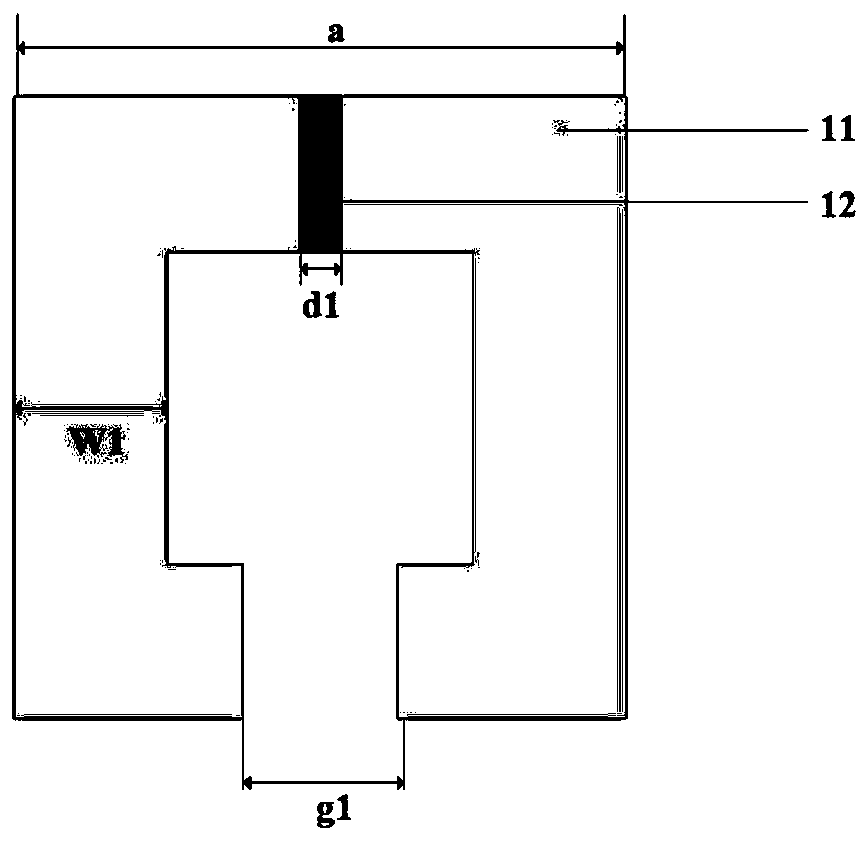
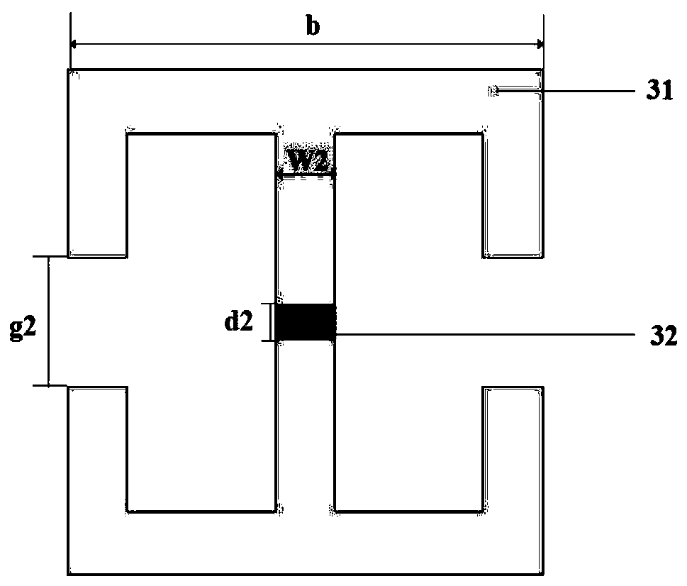
[0032] refer to figure 1 , figure 2 and image 3 :
[0033] A reconfigurable universal metamaterial, including a first resonant unit 1, a dielectric substrate 2 and a second resonant unit 3, the first resonant unit 1 and the second resonant unit 3 are printed on the upper surface of the dielectric substrate 2 respectively and the lower surface;
[0034] The first resonant unit 1 is composed of a single split resonant ring 11 and a varactor diode 12, the single split resonant ring 11 is located on the upper surface of the dielectric substrate 2, and the varactor diode 12 is loaded on the single split resonant ring;
[0035] The second resonant unit 3 is composed of two single-aperture resonant rings 31 with the same structure and varactor diodes 32. The two single-aperture resonant rings 31 with the same structure are located on the lower surface of the dielectric substrate 2, and with respect to the second resonant The geometric center of the unit 3 is distributed symmetr...
Embodiment 2
[0045] Embodiment 2, the structure of this embodiment is identical with the structure of embodiment 1, and following parameter has been adjusted:
[0046] The length and width of the first resonant unit 1 are a=6.2mm, the width w1=1.6mm of the single opening resonant ring 11, the length g1=1.6mm of the opening, the length and width of the second resonant unit 3 are b=6.09mm, The width w2=0.85mm of the two single-slit resonant rings (31) with the same structure, and the length g2=1.6mm of the opening. The length L of the dielectric substrate 2 = 7.09 mm, the width W = 7.09 mm, and the thickness H = 1.2 mm.
Embodiment 3
[0047] Embodiment 3, the structure of this embodiment is the same as that of Embodiment 1, and the following parameters have been adjusted:
[0048] The length and width of the first resonant unit 1 are a=5.8mm, the width w1=1.4mm of the single opening resonant ring 11, the length g1=1.4mm of the opening, the length and width of the second resonant unit 3 are b=5.69mm, The width w2 of the two single-slit resonant rings (31) with the same structure is 0.65 mm, and the length of the opening g2 is 1.4 mm. The length L of the dielectric substrate 2 = 6.69 mm, the width W = 6.69 mm, and the thickness H = 0.8 mm.
[0049] Effect of the present invention can be illustrated by following simulation:
[0050] 1. Simulation model:
[0051] refer to Figure 4
[0052] The reconfigurable metamaterial of Example 1 was modeled in the commercial simulation software HFSS_15.0, and ideal electromagnetic boundaries were set around the metamaterial, wherein the upper and lower boundaries were...
PUM
 Abstract
Description
Claims
Application Information


