Test probe device

A technology for testing probes and auxiliary probes, applied in the directions of measuring devices, measuring electricity, measuring electrical variables, etc., can solve the problems of large probe level, cumbersome operation, poor analysis, etc., and achieve cost saving, easy operation, and test saving. Effects of process and test time

Active Publication Date: 2019-05-10
HEFEI XINSHENG OPTOELECTRONICS TECH CO LTD +1
View PDF7 Cites 2 Cited by
  • Summary
  • Abstract
  • Description
  • Claims
  • Application Information

AI Technical Summary

Problems solved by technology

[0002] In the process of display product development, it is often necessary to test the characteristics of the effective display area of ​​the display panel to resolve defects and analyze the difference between the effective display area and the electrical test area, but the test of the effective display area is relatively troublesome in practice. , requires complex sample preparation, and needs newer probes to test, and the degree of damage to the probes is relatively large, and it takes a lot of manpower and material resources to test samples, and in the actual development of products, each process needs to be based on the detected The characteristics of the effective display area to study different processes, the operation is cumbersome

Method used


Image

  • Test probe device
  • Test probe device
  • Test probe device

Examples


Embodiment Construction

[0055] The following will clearly and completely describe the technical solutions in the embodiments of the present invention with reference to the accompanying drawings in the embodiments of the present invention. Obviously, the described embodiments are only some, not all, embodiments of the present invention. Based on the embodiments of the present invention, all other embodiments obtained by persons of ordinary skill in the art without making creative efforts belong to the protection scope of the present invention.

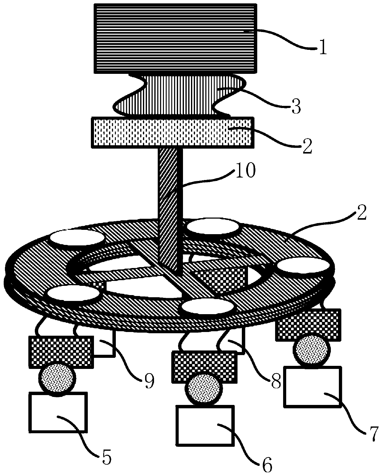
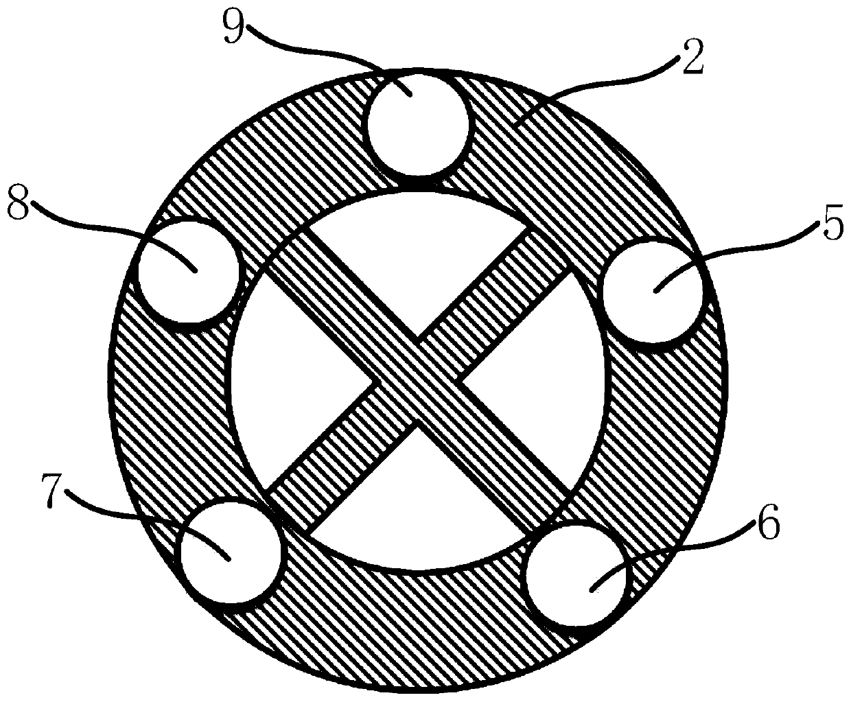
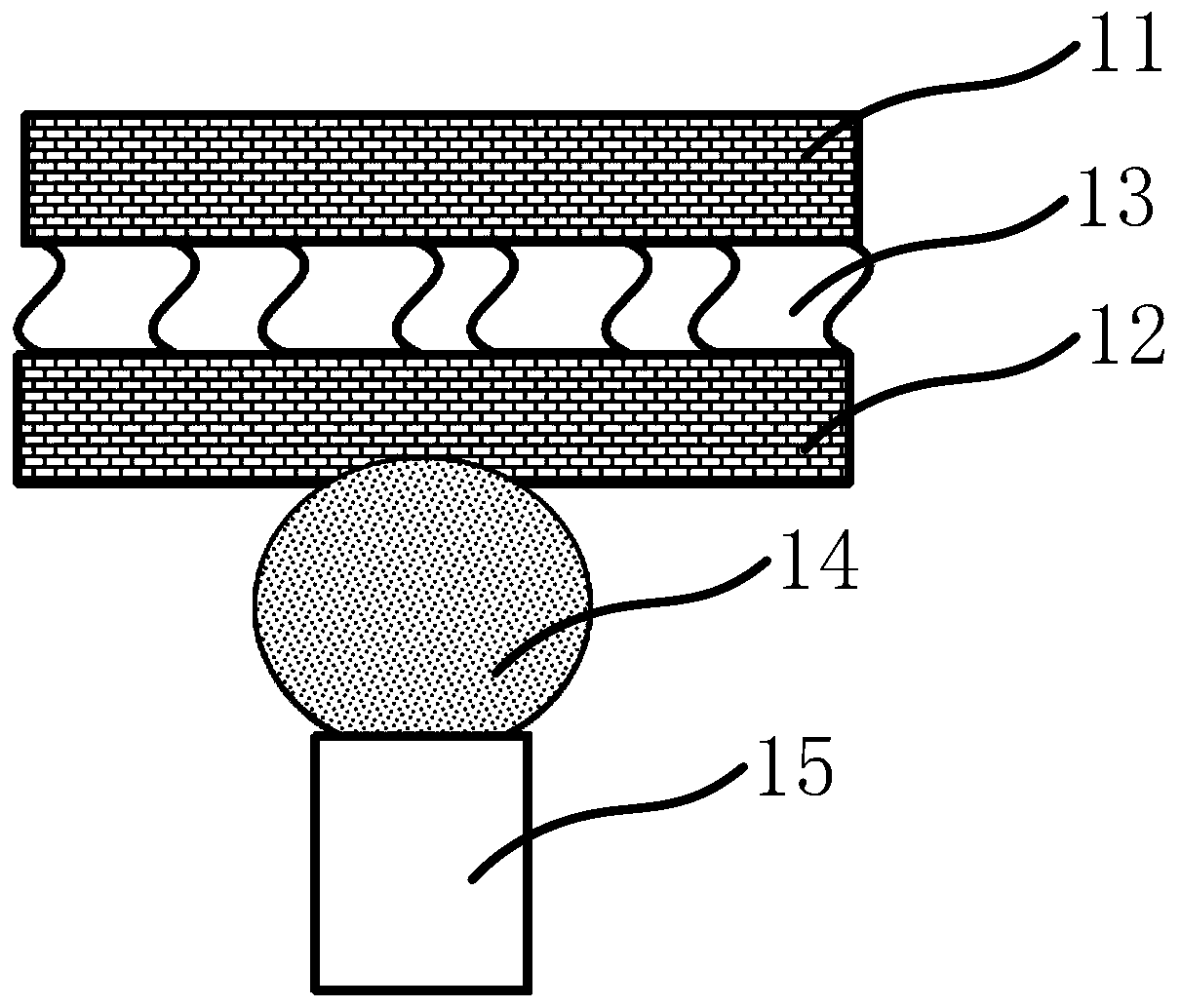
[0056] Please refer to figure 1 , the present invention provides a test probe device, which is used to perform a slice test on the effective display area of ​​a display panel to analyze the characteristics of thin film transistors in the real effective display area, including a bracket 1, a support member 2 that can be lifted and installed on the bracket 1, a drive The support 2 moves relative to the first drive device 3 of the bracket 1, and the test assembly...


PUM


Abstract

The invention relates to the technical field of display equipment, and discloses a test probe device. The test probe device comprises a support, a supporting piece which is mounted on the support in alifting mode, a first driving device for driving the supporting piece to act relative to the support and a test assembly mounted on the supporting piece. The test assembly comprises a mounting plate,a cutting unit, a sucker disc unit, a grinding unit, an auxiliary probe unit and a test probe unit and a second driving device, wherein the cutting unit, the sucker disc unit, the grinding unit, theauxiliary probe unit and the test probe unit are mounted on the mounting plate, and the second driving unit is used for driving the cutting unit, the sucker disc unit, the grinding unit, the auxiliaryprobe unit and the test probe unit to act and to switch between a test station and a non-test station. The test probe device realizes the detection of an effective display area of a display panel, the test process is saved, the test time is shortened, and the cost is saved.

Description

technical field [0001] The invention relates to the technical field of display equipment, in particular to a test probe device. Background technique [0002] In the process of display product development, it is often necessary to test the characteristics of the effective display area of ​​the display panel to resolve defects and analyze the difference between the effective display area and the electrical test area, but the test of the effective display area is relatively troublesome in practice. , requires complex sample preparation, and needs newer probes to test, and the degree of damage to the probes is relatively large, and it takes a lot of manpower and material resources to test samples, and in the actual development of products, each process needs to be based on the detected The characteristics of the effective display area are used to study different processes, and the operation is cumbersome. Contents of the invention [0003] The present invention provides a tes...

Claims


Application Information

Patent Timeline
Patent Type & Authority Applications(China)
IPC IPC(8): G01R1/067B24B49/02B24B49/00B24B41/047B23K26/38B21F11/00B26D1/14B26D1/00
Inventor 王庆贺王东方苏同上汪军丁录科闫梁臣
Owner HEFEI XINSHENG OPTOELECTRONICS TECH CO LTD
Why Eureka
Try Eureka