
A composite rc-ligbt device integrating ldmos and ligbt

A composite type and device technology, applied in the direction of semiconductor devices, electric solid devices, electrical components, etc., can solve the problems of devices not working normally, burning out, excessive local current, etc., and achieve the effect of avoiding the snapback effect

Active Publication Date: 2020-09-01
CHONGQING UNIV OF POSTS & TELECOMM
View PDF4 Cites 0 Cited by
  • Summary
  • Abstract
  • Description
  • Claims
  • Application Information

AI Technical Summary

Problems solved by technology

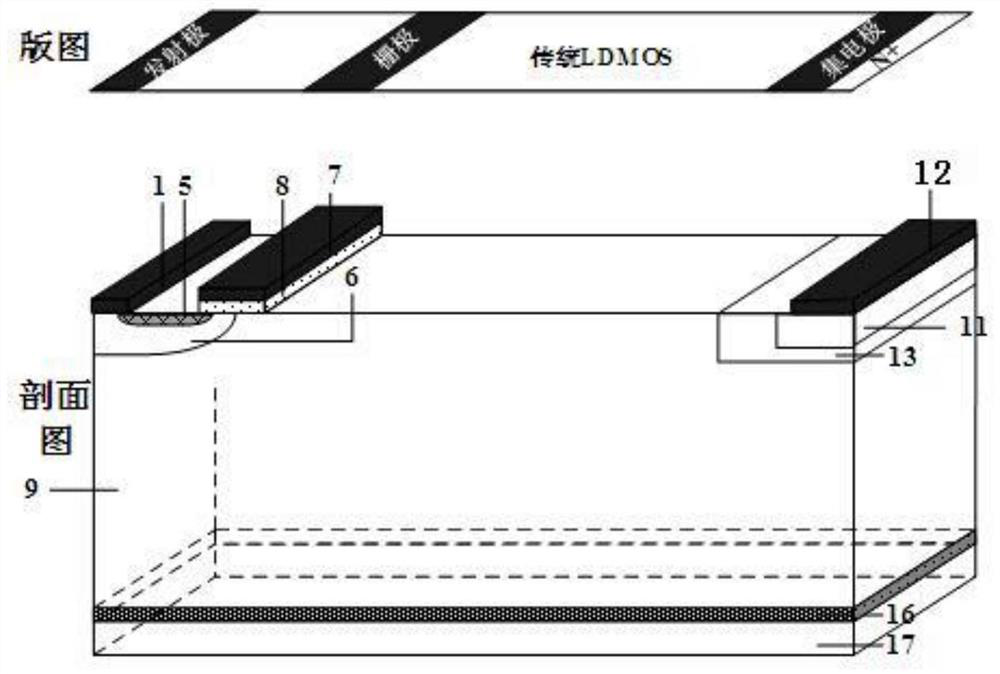
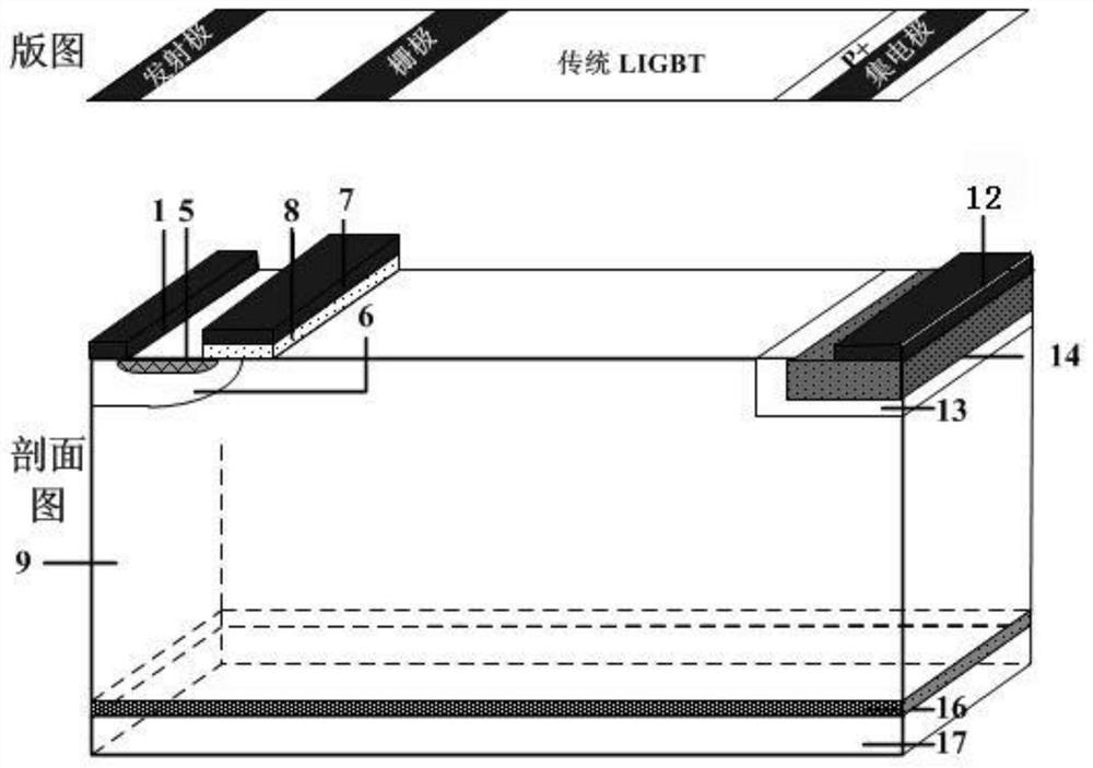
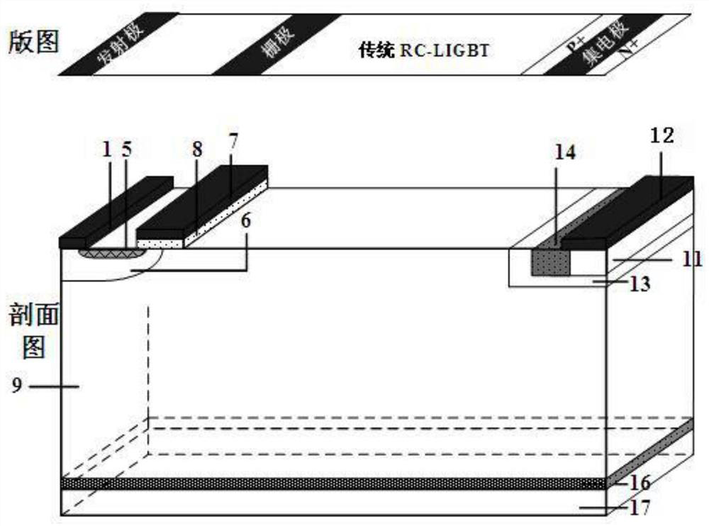
[0004] The traditional RC-LIGBT still has some shortcomings that cannot be ignored in use: for example, in the forward conduction, due to the existence of the collector N-Collector at the initial stage, the electrons injected into the drift region from the emitter will first flow out of the collector through the N-collector. At this moment, only electrons conduct electricity, which is called unipolar conduction mode; as the current flowing through the P-Collector (14) gradually increases, the voltage V between the PN junction formed by the P-Collector and the N-drift region PN will gradually increase when V PN When ≥0.7V, the PN junction is turned on, a large number of holes are injected from the P-Collector into the N-drift region, and the conductance modulation effect occurs, which makes the transistor enter the bipolar conduction mode, and when it is reflected on the forward conduction curve, a " "Voltage rebound phenomenon", the voltage and current on the curve will change suddenly, that is, the negative resistance effect will appear, also known as the snapback effect, this phenomenon will bring a series of problems and affect the reliability of RC-LIGBT devices, such as causing local current If it is too large, the device will not work properly or even burn out, which will lead to the collapse of the entire circuit

Method used


Image

  • A composite rc-ligbt device integrating ldmos and ligbt
  • A composite rc-ligbt device integrating ldmos and ligbt
  • A composite rc-ligbt device integrating ldmos and ligbt

Examples


Embodiment Construction

[0045] Preferred embodiments of the present invention will be described in detail below. For the experimental methods that do not specify specific conditions in the examples, usually follow the conventional conditions or the conditions suggested by the manufacturer.

[0046] The preferred embodiments of the present invention will be described in detail below with reference to the accompanying drawings.

[0047] The cross-sectional structure of a composite RC-LIGBT device integrating LDMOS and LIGBT is shown in Figure 6 Shown: From left to right, it is divided into LDMOS area and LIGBT area. In the LDMOS area, metal collector I12, collector N-Collector 11, N-drift region 9, N-buffer I10, gate oxide layer I4, gate I3, N+ electron emitter I2, emitter 1, P- body 6, below is the dielectric isolation layer 16 and the substrate 17; the LIGBT region is set from right to left metal collector II 15, collector P-Collector 14, N-buffer II 13, N-drift region 9, gate oxide layer II 8, ga...


PUM

PropertyMeasurementUnit
lengthaaaaaaaaaa
lengthaaaaaaaaaa

Abstract

The invention discloses a composite RC-LIGBT (Reverse-Conducting Lateral Insulated Gate Bipolar Transistor) device integrated with an LDMOS (Laterally Diffused Metal Oxide Semiconductor) and an LIGBT(Lateral Insulated Gate Bipolar Transistor). The composite RC-LIGBT device comprises an LDMOS active area and an LIGBT active area which form a left and right symmetrical structure and share the sameemitter. A channel of the LDMOS active area is controlled by a gate I. The channel of the LIGBT active area is controlled by a gate II. A metal collector I is connected with a metal collector II. Thecomposite RC-LIGBT device has the following advantages that when forward switch-on is carried out, snapback effect is eliminated; due to existence of a collector N-Collector in the LDMOS area, when backward switch-on is carried out, the RC-LIGBT composite is enabled to have backward switch-on capability; and blocking effect of a collector P-Collector to a current does not exist, so the backward switch-on capability of the composite RC-LIGBT is superior to that of a conventional RC-LIGBT. The composite RC-LIGBT technology provided by the invention is compatible with a conventional RC-LIGBT technology, only layout design is required, and an additional technology is avoided.

Description

technical field [0001] The invention belongs to the field of power semiconductor devices, in particular to a composite RC-LIGBT device integrating LDMOS and LIGBT. Background technique [0002] LDMOS (Laterally Diffused Metal Oxide Semiconductor) is a commonly used power semiconductor device; in addition to having a drift region that can significantly improve the breakdown voltage of the device; it also has fast switching speed, easy integration, internal The advantages of integrating anti-parallel diodes are widely used in high-voltage and high-frequency fields. However, since LDMOS only conducts electricity through a single electron during forward conduction, it has disadvantages such as low current density and large forward conduction resistance. [0003] LIGBT (Lateral Insulated Gate Bipolar Transistor, Lateral Insulated Gate Bipolar Transistor) was originally transformed from LDMOS. It is a composite semiconductor device that integrates the advantages of both LDMOS and...

Claims


Application Information

Patent Timeline
Patent Type & Authority Patents(China)
IPC IPC(8): H01L27/12H01L29/06H01L29/08
Inventor 陈伟中李顺黄义贺利军秦窈
Owner CHONGQING UNIV OF POSTS & TELECOMM
Learn More