
Semiconductor memory device, operation method thereof, and memory system

A memory controller, memory technology, applied in static memory, digital memory information, information storage, etc., can solve problems such as error yield, adverse effects, increase bits, etc.

Active Publication Date: 2019-05-14
SAMSUNG ELECTRONICS CO LTD
View PDF9 Cites 3 Cited by
  • Summary
  • Abstract
  • Description
  • Claims
  • Application Information

AI Technical Summary

Problems solved by technology

However, reducing size can increase bit errors and adversely affect yield

Method used


Image

  • Semiconductor memory device, operation method thereof, and memory system
  • Semiconductor memory device, operation method thereof, and memory system
  • Semiconductor memory device, operation method thereof, and memory system

Examples


Embodiment Construction

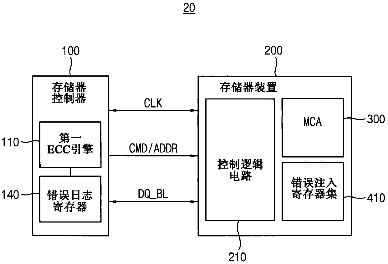
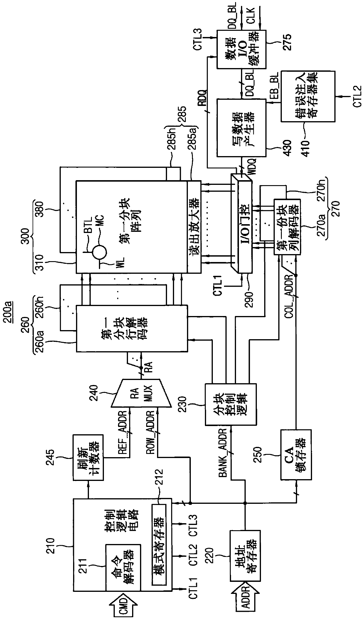
[0025] figure 1 An embodiment of a memory system 20 that may include a memory controller 100 and a semiconductor memory device 200 is shown. The memory controller 100 may control the overall operation of the memory system 20 . The memory controller 100 may control overall data exchange between an external host and the semiconductor memory device 200 . For example, the memory controller 100 may write data into and / or read data from the semiconductor memory device 200 based on a host's request. In addition, the memory controller 100 may issue an operation command to the semiconductor memory device 200 to control the semiconductor memory device 200 .

[0026] For example, the semiconductor memory device 200 may include dynamic memory cells and thus may be a dynamic random access memory (DRAM), double data rate 4 (DDR4) synchronous DRAM (SDRAM), or low power DDR4 (LPDDR4) SDRAM.

[0027] The memory controller 100 sends a clock signal CLK, a command CMD, and an address (signal) ...


PUM


Abstract

The application provides a semiconductor memory device, an operation method thereof, and a memory system. The semiconductor memory device includes a memory cell array, an error injection register set,a data input buffer, a write data generator, and control logic. The error injection register set stores an error bit set, including at least one error bit, based on a first command. The error bit setis associated with a data set to be written in the memory cell array. The data input buffer stores the data set to be written in the memory cell array based on a second command. The write data generator generates a write data set to be written in the memory cell array based on the data set and the error bit set. The control logic controls the error injection register set and the data input buffer.

Description

[0001] Cross References to Related Applications [0002] Korean Patent Application No. 10-2017-0145251 entitled "Semiconductor Memory Device, Memory System, and Method of Operating a Semiconductor Memory Device," filed on Nov. 2, 2017, is hereby incorporated by reference in its entirety. technical field [0003] One or more embodiments herein relate to semiconductor memory devices. Background technique [0004] Various semiconductor memories have been developed. Non-volatile memory includes flash memory. Volatile memory includes dynamic random access memory (DRAM). DRAMs are commonly used for system memory because of their high speed operation and cost efficiency. Efforts are continuing to reduce the size of these devices. However, reducing size can increase bit errors and adversely affect yield. Contents of the invention [0005] According to one or more embodiments, a semiconductor memory device includes: a memory cell array; an error injection register set, which s...

Claims


Application Information

Patent Timeline
Patent Type & Authority Applications(China)
IPC IPC(8): G11C7/10G11C29/44G06F11/10
CPCG11C29/42G06F11/2215G11C29/02G11C29/56004G06F11/1064
Inventor 孙钟弼孙教民
Owner SAMSUNG ELECTRONICS CO LTD
Learn More