Superjunction metal-oxide-semiconductor field effect transistor (MOSFET) containing p-SiC and integrated with Schottky diode

A technology of gate structure and base area, which is applied in the direction of electrical components, electric solid-state devices, circuits, etc., can solve the problems of poor reverse recovery characteristics of body diodes, reduced breakdown voltage of super-junction MOSFETs, and increased reverse recovery charges, etc.

Active Publication Date: 2019-05-14
SICHUAN UNIV
View PDF5 Cites 3 Cited by
  • Summary
  • Abstract
  • Description
  • Claims
  • Application Information

AI Technical Summary

Problems solved by technology

Excess ionized donors in the N-pillar region will significantly increase the highest electric field at the top of the n-pillar region, while excess ionized acceptors in the p-pillar region will significantly increase the highest electric field at the bottom of the p-pillar region, which will lead to the breakdown voltage of the superjunction MOSFET significantly reduce
[0004] Second, the reverse recovery characteristics of the body diode of the super junction MOSFET are relatively poor
However, this approach increases the reverse recovery charge and also increases the on-resistance

Method used


Image

  • Superjunction metal-oxide-semiconductor field effect transistor (MOSFET) containing p-SiC and integrated with Schottky diode
  • Superjunction metal-oxide-semiconductor field effect transistor (MOSFET) containing p-SiC and integrated with Schottky diode
  • Superjunction metal-oxide-semiconductor field effect transistor (MOSFET) containing p-SiC and integrated with Schottky diode

Examples


Embodiment Construction

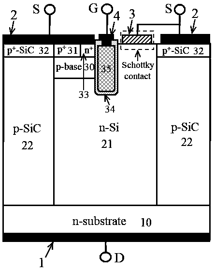
[0031]The present invention will be described in detail below in conjunction with the accompanying drawings.

[0032] figure 1 It is a trench gate super junction MOSFET of the present invention. figure 1 The main difference between the structure and the ordinary super junction MOSFET is that the p-column region (p-SiC region 22) uses silicon carbide (SiC) material, and the upper surface of the n-column region (n-Si region 21) is in contact with the conductor 3 Form a Schottky contact (Schottky Contact) and connect it to the source S through a wire. figure 1 The main advantages of the structure are twofold: first, the breakdown voltage is less susceptible to charge balance; second, the body diode has less reverse recovery charge, resulting in less current and voltage oscillations. These two advantages are explained separately below.

[0033] In forward withstand voltage, the highest electric field in the n-pillar region (n-Si region 21 ) appears at the top, and the highest e...


PUM


Abstract

The invention provides a superjunction metal-oxide-semiconductor field effect transistor (MOSFET) device. A second type of semiconductor area of the second conductive type in a voltage withstanding layer of the MOSFET device can be made of silicon carbide materials, a first type of semiconductor area of the first conductive type in the voltage withstanding layer of the MOSFET device can be made ofsilicon materials, at least part of the upper surface of the first type of semiconductor area of the first conductive type in the voltage withstanding layer makes contact with a conductor to form a Schottky contact electrode, and the Schottky contact electrode is connected with a source electrode through a wire. Compared with a common superjunction MOSFET device, the breakdown voltage of the superjunction MOSFET device is more not prone to being affected by charge non-equilibrium, and the reverse recovery characteristics of a diode are better.

Description

technical field [0001] The invention belongs to semiconductor devices, especially semiconductor power devices. Background technique [0002] Superjunction Metal-Oxide-Semiconductor Field Effect Transistor (Superjunction Metal-Oxide-Semiconductor Field Effect Transistor, Superjunction MOSFET) is a widely used power switching device with superior performance. The super-junction MOSFET adopts a voltage-resistant structure in which n-column regions / p-column regions are arranged alternately, which can enable the n-column region and p-column region to obtain a higher breakdown voltage at a higher doping concentration. Therefore, the on-resistance of super-junction MOSFETs is usually relatively low. However, super-junction MOSFETs also have two major disadvantages. [0003] First, the super-junction MOSFET needs to precisely control the doping concentration of the n-column region and the p-column region to achieve charge balance (that is, the total number of effective donor impur...

Claims


Application Information

Patent Timeline
Patent Type & Authority Applications(China)
IPC IPC(8): H01L29/06H01L29/16H01L29/78H01L29/872H01L27/06
Inventor 黄铭敏
Owner SICHUAN UNIV
Why Eureka
Try Eureka