Processing method and device for silicon wafer

A treatment method and technology of treatment device, which are applied in the directions of cleaning methods and utensils, cleaning methods using liquids, chemical instruments and methods, etc., can solve the problems of deterioration of particle quality, increase of secondary pollution, pollution, etc., and reduce secondary pollution. , Enhance removal ability, improve the effect of cleaning effect

Inactive Publication Date: 2019-05-17
XIAN ESWIN SILICON WAFER TECH CO LTD
View PDF12 Cites 4 Cited by
  • Summary
  • Abstract
  • Description
  • Claims
  • Application Information

AI Technical Summary

Problems solved by technology

Therefore, as far as the first silicon wafer that finishes final polishing is concerned, it will stand by for a long time in the unloading tank, so the possibility of secondary pollution after exposure will increase
[0006] like Figure 2a , Figure 2b and Figure 2c As shown, the silicon wafer transport box 8 installed in the unloading tank 7 is horizontal, and the silicon wafer transport box 8 is provided with a plurality of draw-in slots, and the silicon wafer 9 can be placed in the draw-in slots, and the silicon wafers in the silicon wafer transport box 8 The carrying surface is parallel to the horizontal plane. Whenever the silicon wafers 9 complete the final polishing process and are loaded into the silicon wafer delivery box 8 one by one, the silicon wafer delivery box 8 loads the silicon wafers 9 on the outside of the unloading tank 7 where the water is exposed. However, the unloading tank 7 The more the number of times the inner silicon wafer transport box 8 is exposed to the outside of th

Method used


Image

  • Processing method and device for silicon wafer
  • Processing method and device for silicon wafer
  • Processing method and device for silicon wafer

Examples


Example Embodiment

[0046] In order to make the purpose, technical solutions and advantages of the embodiments of the present invention more clear, the following will clearly and completely describe the technical solutions of the embodiments of the present invention in conjunction with the drawings of the embodiments of the present invention. Apparently, the described embodiments are some, not all, embodiments of the present invention. All other embodiments obtained by those skilled in the art based on the described embodiments of the present invention belong to the protection scope of the present invention.

[0047] The method for processing a silicon wafer according to an embodiment of the present invention will be specifically described below.

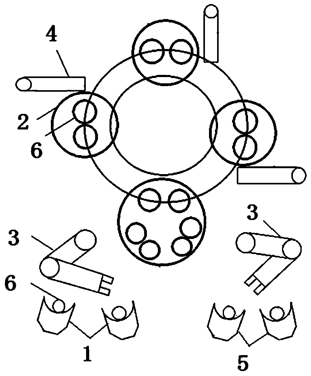
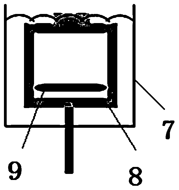
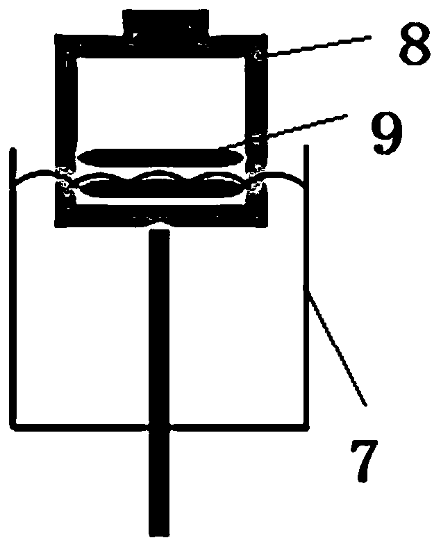
[0048] According to the silicon wafer processing method of the embodiment of the present invention, the silicon wafer transport box is placed in the unloading tank filled with immersion liquid and in an overflow state, the interaction surface of the sili...


PUM


Abstract

The invention provides a processing method and device for a silicon wafer. The processing method of the silicon wafer comprises the steps that a silicon wafer conveyor box is placed in a unloading tank containing an immersion solution and in the overflow state, the interaction surface of the silicon wafer conveyor box is parallel to the horizontal surface of the silicon wafer conveyor box, the bearing surface for bearing a silicon wafer in the silicon wafer conveyor box is perpendicular to the horizontal surface, after the final polishing of the silicon wafer is completed, and the silicon wafer is vertically loaded into the wafer conveyor box and immerse in the immersion solution. According to the processing method of the silicon wafer, after the final polishing of the silicon wafer is completed, the silicon wafer can be vertically loaded into the silicon wafer conveyor box and immersed in the immersion solution, so that the silicon wafer in the silicon wafer conveyor box is avoided tocome out when the silicon wafer is finally polished and loaded into the silicon wafer conveyor box, and the etch caused by residual slurry is reduced; and the processing method of the silicon wafer can be realized through the silicon wafer processing device, the secondary pollution of the silicon wafer is effectively reduced, and the cleaning effect is improved.

Description

technical field [0001] The invention relates to the technical field of silicon wafers, in particular to a silicon wafer processing method and device. Background technique [0002] In the polishing process of silicon wafers, the general polishing process is carried out in the order of double-sided polishing→cleaning→edge polishing→cleaning→final polishing. According to needs, it can also follow the order of edge polishing→cleaning→double-sided polishing→cleaning→ The polishing process is carried out in the order of final polishing. In addition, in order to strengthen the monitoring of wafer quality in the polishing process, a flatness measurement process and an edge inspection process can also be added. Final polishing is the process of performing final polishing on the front side of silicon wafers that have been double-sided and edge-polished by using polishing pads, polishing slurries, stencil components, and other chemicals. Thus, it should be possible to ultimately dete...

Claims


Application Information

Patent Timeline
IPC IPC(8): B24B29/02B08B3/04B08B3/02
Inventor 具成旻崔世勋李昀泽白宗权
Owner XIAN ESWIN SILICON WAFER TECH CO LTD
Why Eureka
Try Eureka