
Non-contact card manufacturing device and non-contact card manufacturing method

A contactless card and manufacturing equipment technology, applied in welding equipment, manufacturing tools, metal processing equipment, etc., can solve the problems of high labor costs, low quality of contactless cards, and low level of automatic manufacturing of contactless cards, and avoid Effects on the Chip Surface

Active Publication Date: 2019-05-21
SHANGHAI ORIENTAL MAGNETIC CARD ENG
View PDF15 Cites 1 Cited by
  • Summary
  • Abstract
  • Description
  • Claims
  • Application Information

AI Technical Summary

Problems solved by technology

[0003] The technical problem to be solved by the present invention is to provide a contactless Card manufacturing equipment and contactless card manufacturing method

Method used


Image

  • Non-contact card manufacturing device and non-contact card manufacturing method
  • Non-contact card manufacturing device and non-contact card manufacturing method
  • Non-contact card manufacturing device and non-contact card manufacturing method

Examples


Embodiment 1

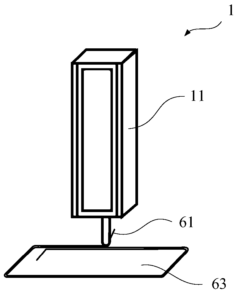
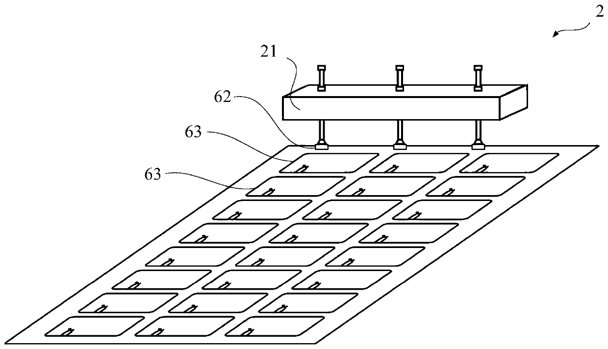
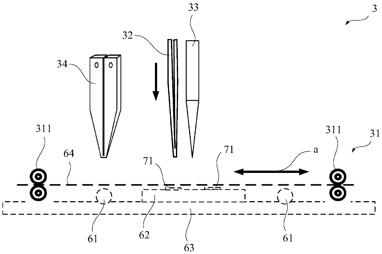
[0080] Such as figure 1 , figure 2 , image 3 and Figure 4 As shown, the present invention provides a contactless card manufacturing equipment, which is used to manufacture contactless cards. The contactless card manufacturing equipment includes an antenna implantation device 1, a chip fixing device 2, a pin welding device 3 and a transmission device 4 . Among them, the antenna implantation device 1 is used to implant the copper wire 61 into the card making substrate 63, and the chip fixing device 2 is used to place the chip 62 in a corresponding fixed position on the card making substrate 63 to form a non- Contact the antenna of the card, and the pin welding device 3 is used to weld the wire 64 to the pin 621 of the chip 62 and the copper wire 61 to make the conduction between the chip 62 and the copper wire 61, and the transmission device 4 is used to connect the wire 62 to the copper wire 61. The card making base material 63 is transported between the antenna implanti...

Embodiment 2

[0111] Such as Figure 6 As shown, this embodiment also provides a contactless card manufacturing equipment, which has roughly the same structure as the contactless card manufacturing equipment provided in Embodiment 1, the difference is that in this embodiment, the contactless card manufacturing equipment The pin welding device 3 of the equipment includes two welding pins 32 arranged side by side, and the cutting mechanism 33 is located between the two welding pins 32 . This pin welding device 3 can be applied to the situation that the chip 62 has more than two pins 621, and the wire 64 can be welded on two pins 621 wherein, and these two pins 621 are drawn out through the wire 64 simultaneously. . Specifically, by setting two welding pins 32 on the pin welding device 3, these two welding pins 32 can simultaneously weld the wire 64 straightened and fixed by the fixing mechanism 31 on the two pins 621 of the chip 62. , and the cutting mechanism 33 is located between the two ...


PUM


Abstract

The invention discloses a non-contact card manufacturing device and a non-contact card manufacturing method. The non-contact card manufacturing device comprises an antenna implanting device used for implanting copper wires into a card manufacturing base material, a chip fixing device used for placing a chip in a fixed position of the card manufacturing base material, a pin welding device used forwelding the two ends of a lead wire to pins and copper wires of the chip, and a conveying device used for conveying the card manufacturing base material among the antenna implanting device, the chip fixing device and the pin welding device. According to the non-contact card manufacturing device and the non-contact card manufacturing method, the conveying device is used for conveying the card manufacturing base material, so that the card manufacturing base material can be conveyed among the devices corresponding to all processing links; and the required chip and antenna are arranged on the surface based on the card manufacturing base material, so that the manufacturing of a non-contact card is more automated and standardized, and the labor cost of the manufacturing is reduced.

Description

technical field [0001] The invention relates to a non-contact card manufacturing equipment and a non-contact card manufacturing method. Background technique [0002] In the prior art, operators use various equipment to install copper wires, chips, etc. on the corresponding positions of the card making substrate to make a contactless card. Due to the low level of automation in the manufacture of contactless cards, more labor costs will be incurred in the manufacturing process, and there are differences in consistency between the produced contactless cards, which makes it difficult to improve the overall quality and cannot produce high-quality cards. contactless card products. Contents of the invention [0003] The technical problem to be solved by the present invention is to provide a contactless Card manufacturing equipment and contactless card manufacturing method. [0004] The present invention solves the above technical problems through the following technical soluti...

Claims


Application Information

Patent Timeline
Patent Type & Authority Applications(China)
IPC IPC(8): H01L21/677H01L21/50H01L21/52H01Q1/22G06K19/077
CPCG06K19/077H01L21/677H01Q1/22H01L21/50H01L21/52B23K1/0016B23K1/19B23K1/20B23K2101/38B23K3/087B23K2101/36G06K19/07758G06K19/07773
Inventor 李晓东
Owner SHANGHAI ORIENTAL MAGNETIC CARD ENG
Learn More