Memory and forming method thereof, and selection method of storage unit of memory

A memory and storage string technology, applied in electrical components, electric solid-state devices, semiconductor devices, etc., can solve the problems of reducing the density of memory storage units, occupying a large memory chip area, and complicated selection methods of storage units, so as to avoid structural changes , Improve reliability and avoid leakage

Pending Publication Date: 2019-05-21
YANGTZE MEMORY TECH CO LTD
View PDF5 Cites 22 Cited by
  • Summary
  • Abstract
  • Description
  • Claims
  • Application Information

AI Technical Summary

Problems solved by technology

[0004] In the prior art, the memory cells of the above-mentioned 3D NAND memory need to be divided into multiple memory blocks through the partition wall that runs through the memory stack structure, and then the memory cells at specific positions are selected throug

Method used


Image

  • Memory and forming method thereof, and selection method of storage unit of memory
  • Memory and forming method thereof, and selection method of storage unit of memory
  • Memory and forming method thereof, and selection method of storage unit of memory

Examples


Embodiment Construction

[0026] Specific implementations of the memory provided by the present invention, its forming method, and the method for selecting storage units of the memory will be described in detail below in conjunction with the accompanying drawings.

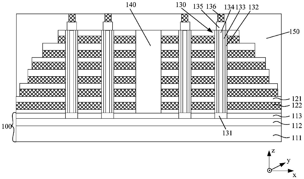
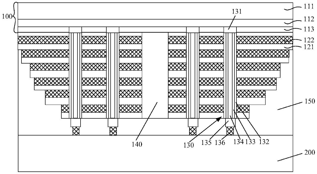
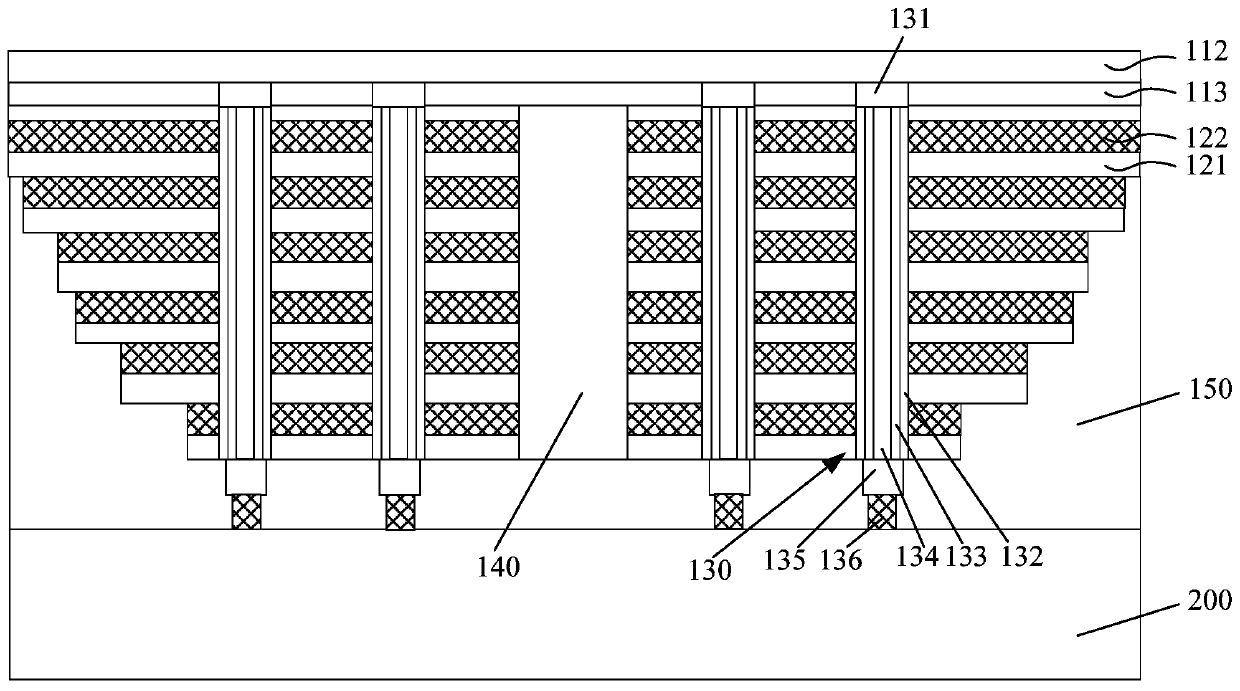
[0027] Please refer to figure 1 , providing a storage substrate, the storage substrate includes: a substrate 100 and a storage stack structure formed on the front surface of the substrate; a channel column structure 130 penetrating to the surface of the substrate is also formed in the storage stack structure, a penetrating The isolation wall 140 between the initial stack structure and the surface of the substrate.

[0028] The substrate 100 may be a semiconductor material, such as a single crystal silicon substrate, a single crystal germanium substrate, an SOI (silicon on insulator) substrate or a GOI (germanium on insulator) substrate, etc., and the substrate 100 may also be For n-type doping or p-type doping. A person skilled in the ar...


PUM


Abstract

The invention relates to a memory and a forming method thereof, and a selection method of a storage unit of a memory. The forming method of the memory comprises the following steps: a storage base isprovided; the storage base comprises a substrate and a storage stacking structure formed on the front side of the substrate; a channel column structure and a separation wall for penetrating the storage stacking structure into the surface of the substrate are formed in the storage stacking structure; the back of the substrate is thinned; a dielectric layer is formed on the thinned back of the substrate; a contact part that penetrates the dielectric layer and is connected to the bottom of the channel column structure is formed; source lines are formed on the dielectric layer; and, the contact part located in the same one row is connected with the same one source line. The method provided by the invention is helpful for improving the storage density of the memory.

Description

technical field [0001] The invention relates to the technical field of semiconductors, in particular to a memory, a method for forming the same, and a method for selecting memory cells of the memory. Background technique [0002] In recent years, the development of flash memory (Flash Memory) is particularly rapid. The main feature of flash memory is that it can keep stored information for a long time without power on, and has the advantages of high integration, fast access speed, easy erasing and rewriting, etc. Has been widely used. In order to further increase the bit density (Bit Density) of the flash memory while reducing the bit cost (Bit Cost), three-dimensional flash memory (3D NAND) technology has been developed rapidly. [0003] The existing 3D NAND memory includes a substrate and a memory stack structure formed on the surface of the substrate. A channel column structure penetrating to the surface of the substrate is formed in the memory stack structure to form a...

Claims


Application Information

Patent Timeline
IPC IPC(8): H01L27/11563H01L27/11578H01L27/11582
Inventor 刘毅华刘峻范鲁明
Owner YANGTZE MEMORY TECH CO LTD
Why Eureka
Try Eureka