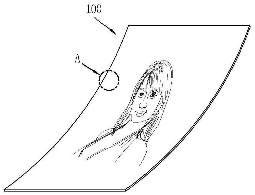
Display device using semiconductor light emitting device and manufacturing method thereof
A technology for display devices and light-emitting devices, applied in semiconductor devices, electrical solid devices, identification devices, etc., can solve problems such as poor adhesion of wavelength conversion layers and color filters, and compensate for the weakening and reducing of adhesion. Gap, separation prevention effect
- Summary
- Abstract
- Description
- Claims
- Application Information
AI Technical Summary
Problems solved by technology
Method used
Image

Examples
Embodiment Construction
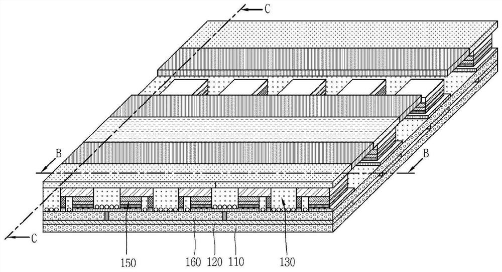
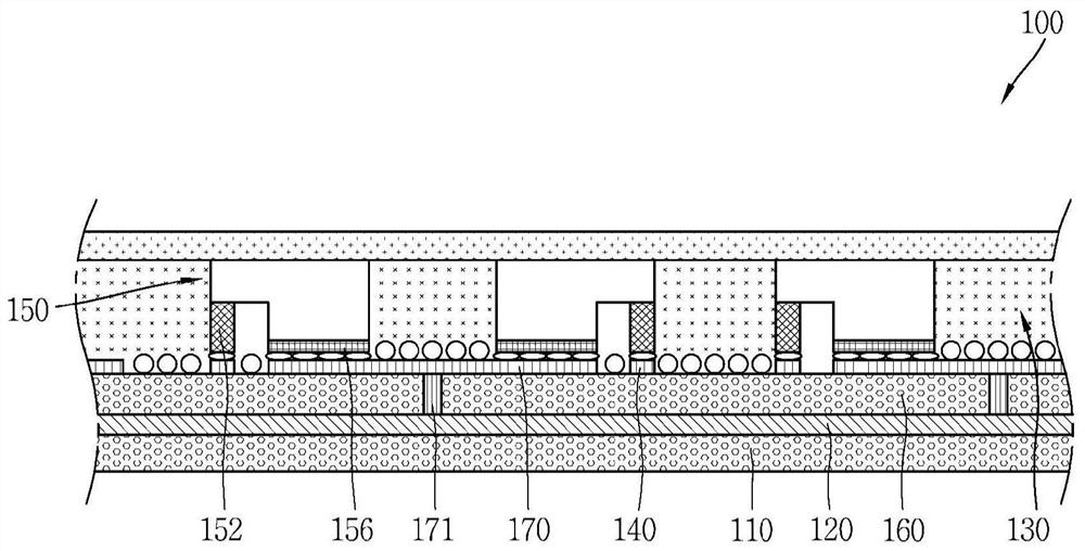
[0040] Hereinafter, embodiments disclosed herein will be described in detail with reference to the accompanying drawings, and the same reference numerals will be used to designate the same or similar elements regardless of the numerals in the drawings, and redundant descriptions thereof will be omitted. . The suffixes "module" and "unit" used for constituent elements disclosed in the following description are merely intended to facilitate description of this specification, and the suffixes themselves do not give any special meaning or function. In describing the present disclosure, if a detailed description of a related known function or construction is considered to unnecessarily divert the gist of the present disclosure, such description has been omitted but will be understood by those skilled in the art. In addition, it should be noted that the accompanying drawings are only illustrated to easily explain the concept of the present invention, and thus, they should not be con...
PUM
| Property | Measurement | Unit |
|---|---|---|
| thickness | aaaaa | aaaaa |
Abstract
Description
Claims
Application Information
PatSnap Eureka turns technology decisions into work you can execute. Powered by our Innovation Knowledge Graph, it runs expert workflows across engineering, life sciences, materials and intellectual property. Get your review-ready output in minutes.


