Semiconductor device for correcting warpage of plastic packaging panel and correction method

A semiconductor and flat panel technology, which is applied in semiconductor/solid-state device manufacturing, electrical components, circuits, etc., can solve problems such as unevenness and warping of plastic-encapsulated flat panels, and achieve the effect of protecting integrity

Inactive Publication Date: 2019-05-24
NAT CENT FOR ADVANCED PACKAGING
View PDF8 Cites 3 Cited by
  • Summary
  • Abstract
  • Description
  • Claims
  • Application Information

AI Technical Summary

Problems solved by technology

[0006] Therefore, the technical problem to be solved by the present invention is to overcome the problem that the semiconductor device used to correct the warped plastic-encapsulated flat panel in the prior art is easy to damage the bare chip on the plastic-enclosed flat panel or the corrected plastic-enclosed flat panel is still uneven and still has various types of defects. Various warping technical defects, so as to provide a method for correcting integrated circuits that is not easy to damage the bare chip during the correction process, and the flatness of the plastic-encapsulated flat plate after correction is good, and the flatness that fully meets the requirements of various semiconductor processes is provided. Semiconductor device and correcting method for warpage of plastic-encapsulated flat plate of chip

Method used


Image

  • Semiconductor device for correcting warpage of plastic packaging panel and correction method
  • Semiconductor device for correcting warpage of plastic packaging panel and correction method
  • Semiconductor device for correcting warpage of plastic packaging panel and correction method

Examples


Embodiment 1

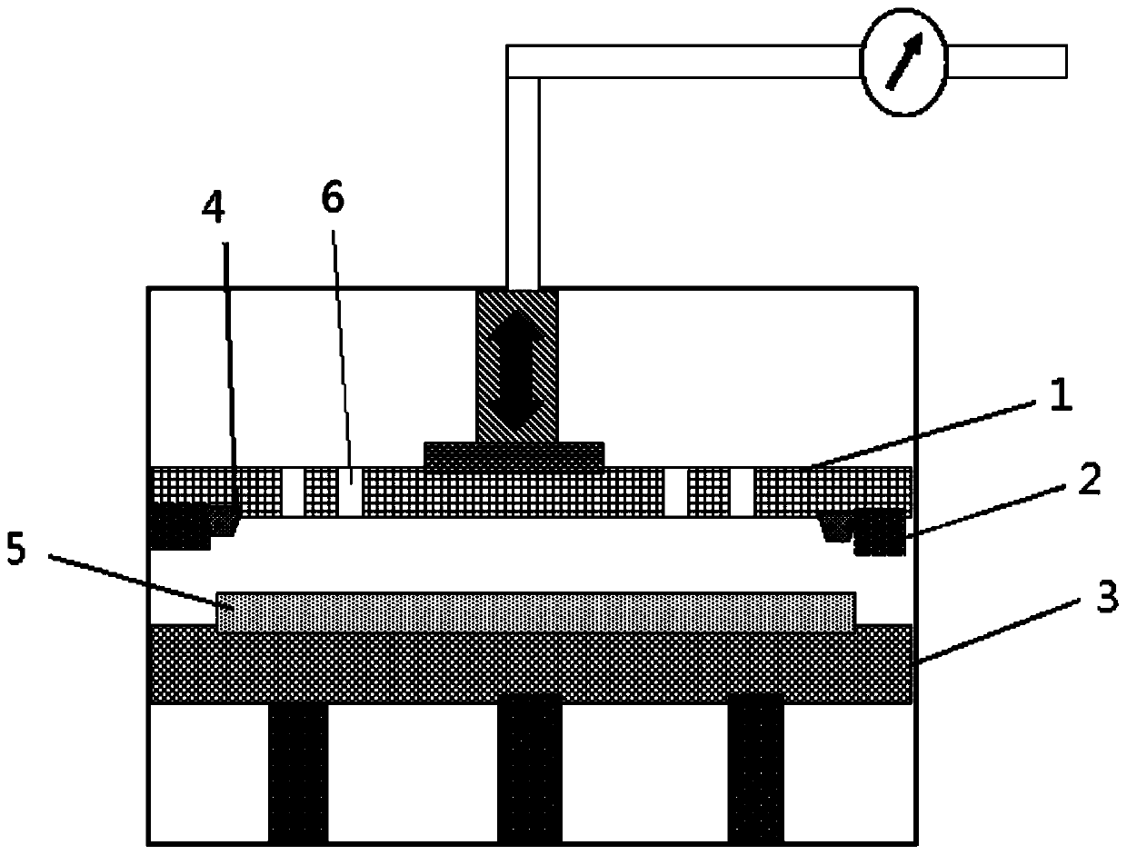
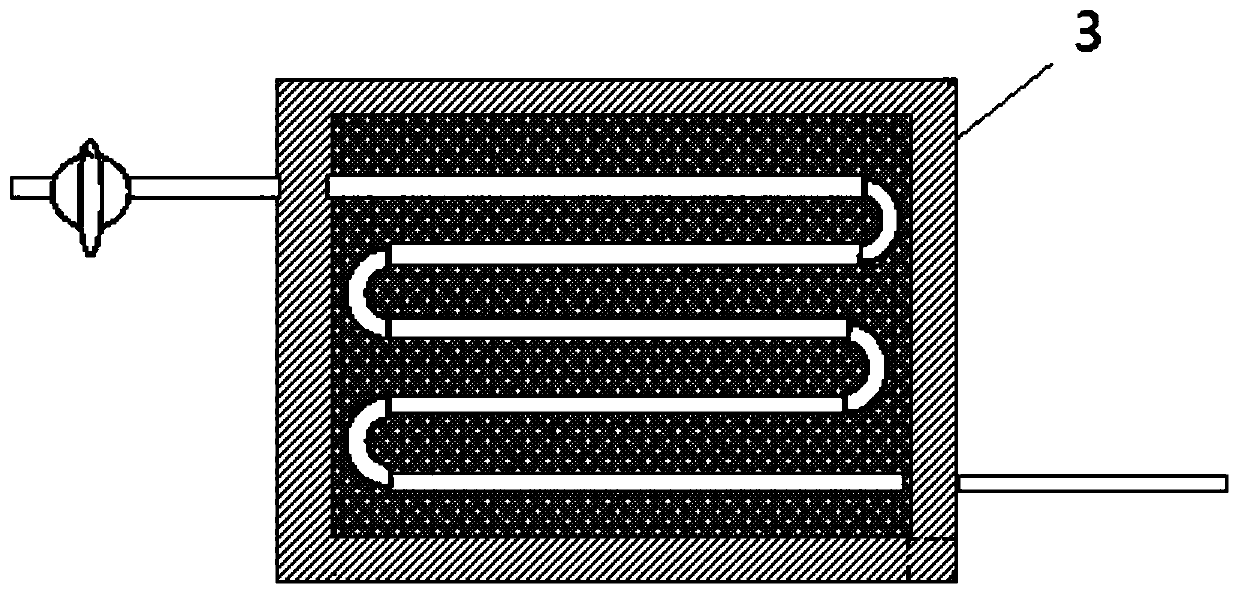
[0046] Such as figure 1 -3 shows a specific implementation of the semiconductor device used to correct the warpage of the plastic-encapsulated flat plate containing the integrated circuit chip involved in the present invention, which includes a carrying structure 3, a vacuum channel, a pressing structure, a protective ring 2 and a heating structure.

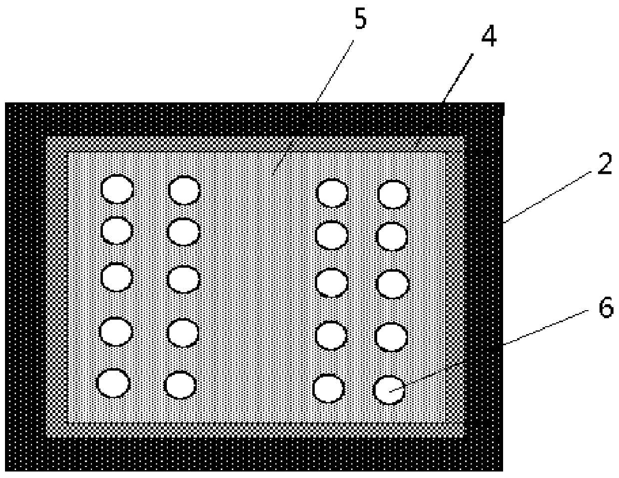
[0047] In this embodiment, the carrying structure 3 includes a carrying area for carrying the plastic-encapsulated flat panel 5 , and the carrying area is arranged on a plane. The surface of the bearing area needs to be polished to ensure that the back of the plastic-encapsulated flat panel will not be scratched when the warpage is corrected.

[0048] In this embodiment, a vacuum channel is provided on the carrying structure 3 and communicated with the carrying area to apply a vacuum to the gap between the plastic sealing plate 5 and the carrying area, thereby ensuring that the plastic sealing plate The back can be flatly attac...

Embodiment 2

[0069] The present invention provides a method for correcting a plastic-encapsulated flat panel using the semiconductor device described in Embodiment 1, which includes the following steps:

[0070] Place the plastic-encapsulated flat panel 5 on the bearing area and heat the plastic-encapsulated flat panel 5; the pressing structure moves toward the plastic-enclosed flat panel 5 and makes the pressing end 4 contact with the plastic-enclosed flat panel 5 to apply pressure , applying a vacuum to the gap between the plastic-encapsulated flat panel 5 and the bearing area, so that the plastic-enclosed flat panel 5 closely adheres to the surface of the loaded area; finally, cooling the flattened plastic-enclosed flat panel 5 .

[0071] The warped plastic flat plate of the fan-out package to be corrected is sent to the cavity of the semiconductor device and placed on the surface of the loading area accurately. The loading structure is preheated to the temperature required by the proces...


PUM


Abstract

The invention relates to the technical field of advanced packaging technologies for integrated circuits, and specifically relates to a semiconductor device for correcting warpage of a plastic packaging panel containing an integrated circuit chip and a correction method. The semiconductor device comprises a load-bearing structure, a vacuum channel, a pressing structure and a heating structure, wherein the load-bearing structure is used for bearing a load-bearing area of the plastic packaging panel, and the load bearing area is set to be a plane; the vacuum channel is arranged on the load-bearing structure, communicated with the load-bearing area, and used for applying vacuum to a gap between the plastic packaging panel and the load-bearing area; the pressing structure is arranged above theload-bearing structure and moves back and forth in a direction perpendicular to the load-bearing area, the pressing structure is provided with a pressing end which is arranged corresponding to the plastic packaging panel and used for applying correction pressure to a part without a bare chip of the plastic packaging panel, and the contact surface between the pressing end and the plastic packagingpanel is a plane; and the heating structure is arranged on the load-bearing structure and/or pressing structure and used for heating the plastic packaging panel. The semiconductor device of the invention is not easy to damage the bare chip during correction and is good in correction effect.

Description

technical field [0001] The invention relates to the technical field of advanced packaging of integrated circuits, in particular to a semiconductor device and a correction method for correcting the warpage of a plastic-encapsulated flat plate containing an integrated circuit chip. Background technique [0002] Due to its own characteristics, board-level fan-out packaging has high production capacity. In recent years, it has been concerned by the integrated circuit packaging and testing industry. Foot small chip package, its production cost is undoubtedly a huge attraction. [0003] In fan-out packaging, it is an essential step to reconfigure wafers or large-size flat plates by plastic encapsulation. Usually, the chip is reassembled into a well-tested chip (known-gooddie) that can continue the process according to the package design layout. Integrated wafer or flat panel. However, due to the difference in physical parameters such as elastic modulus and thermal expansion coef...

Claims


Application Information

Patent Timeline
Patent Type & Authority Applications(China)
IPC IPC(8): H01L21/67H01L21/683
Inventor 姚大平
Owner NAT CENT FOR ADVANCED PACKAGING
Why Eureka
Try Eureka