Semiconductor chip test system and method

A chip testing and semiconductor technology, applied in the testing field of semiconductor chip testing interface devices, can solve problems such as expensive and time-consuming testing, and achieve the effects of reducing quantity, shortening downtime, and reducing costs

Active Publication Date: 2019-05-31
INTEL PROD CHENGDU CO LTD +1
View PDF8 Cites 1 Cited by
  • Summary
  • Abstract
  • Description
  • Claims
  • Application Information

AI Technical Summary

Problems solved by technology

But such dedicated inspection equipment is expensive, and removing the test interface device from the test system requires stoppin

Method used


Image

  • Semiconductor chip test system and method
  • Semiconductor chip test system and method
  • Semiconductor chip test system and method

Examples


Example Embodiment

[0015] In the following description, several specific details are set forth. However, embodiments as described herein may be practiced without some of the specific details. In particular embodiments, well-known structures and techniques have not been shown in detail in order not to obscure the understanding of the description.

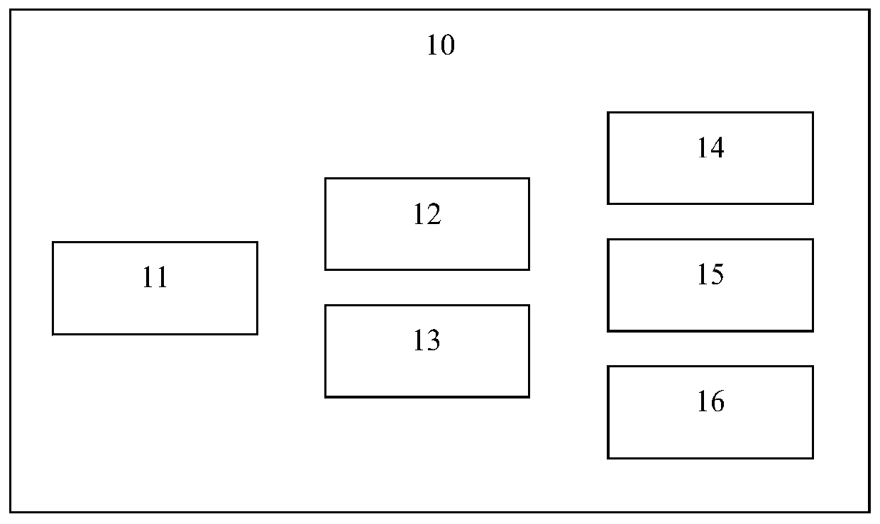
[0016] figure 1 A block diagram of a semiconductor chip testing system 10 according to one embodiment of the present invention is shown. The semiconductor chip test system 10 includes a robot arm 11 , a test interface device 12 , a test circuit 13 , an image acquisition device 14 , a processor 15 and a controller 16 .

[0017] The robotic arm 11 is used to pick up a semiconductor chip to be tested, such as a wafer to be tested or a packaged die, and place the semiconductor chip in the test interface device 12 or remove it from the test interface device 12 . In some cases, the robot arm 11 may be omitted from the semiconductor chip testing system 10 ...


PUM


Abstract

The present invention provides a semiconductor chip test system. The system comprises: a test circuit; a test interface device comprising a plurality of probes to provide electrical connection betweena semiconductor chip to be tested and the test circuit so as to allow the test circuit to test the semiconductor chip to be tested; an image obtaining device configured to obtain images of the test interface device, wherein the probes are shown in the images; and a processor configured to detect the test interface device based on the obtained image to determine the possible defects in the test interface device and generate output signals based on the determination result of the defects. The detection for the test interface device is provided during the test of the semiconductor chip to prevent the test interface device from being taken out from the semiconductor chip test system as far as possible for detection so as to shorten the downtime of the semiconductor chip test system and save the cost.

Description

technical field [0001] The invention relates to the field of semiconductor chip testing, in particular to the detection of semiconductor chip testing interface devices. Background technique [0002] Semiconductor circuits are initially manufactured in the form of a wafer, which is a circular silicon chip on which many independent circuits are formed. Each such circuit can be called a die. These dies are cut and packaged into different forms through a dicing process to form common semiconductor packages. [0003] In the above-mentioned semiconductor manufacturing process, it is necessary to test the semiconductor chip. Common tests include wafer test and post-package test. The current automatic test system includes a manipulator, a test interface device, a test circuit and a controller. The robotic arm picks up the semiconductor chip to be tested, such as a wafer or packaged die, etc., and places the semiconductor chip in the corresponding chip test socket in the test inte...

Claims


Application Information

Patent Timeline
IPC IPC(8): G01N21/95G01R31/26
Inventor 牟赟
Owner INTEL PROD CHENGDU CO LTD
Why Eureka
Try Eureka