
A kind of preparation method of Gan-based light-emitting diode epitaxial wafer

A technology of light-emitting diodes and epitaxial wafers, applied in semiconductor/solid-state device manufacturing, semiconductor devices, electrical components, etc., can solve problems such as destroying AlN and GaN lattice matching, affecting the crystal quality of epitaxial wafers, etc., to improve the effective radiation recombination probability , reduce defects, and improve crystal quality

Active Publication Date: 2021-06-11
HC SEMITEK ZHEJIANG CO LTD
View PDF0 Cites 0 Cited by
  • Summary
  • Abstract
  • Description
  • Claims
  • Application Information

AI Technical Summary

Problems solved by technology

[0004] In the process of realizing the present invention, the inventors have found that the prior art has at least the following problems: in the preparation process of the epitaxial wafer, although the AlN buffer layer can relieve the sapphire substrate (AlN 2 o 3 ) and the GaN material, but because the preparation methods of the AlN buffer layer and the GaN epitaxial layer are different, it is necessary to transport the AlN template to the MOCVD equipment for the production of the GaN epitaxial layer. In the process of transportation and use, the AlN template will inevitably come into contact with the air, and a thin layer of Al will be formed on the surface of the AlN template. 2 o 3 thin film, this layer of thin film will greatly destroy the lattice matching between AlN and GaN, and affect the crystal quality of the epitaxial wafer

Method used

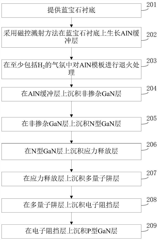

Image

  • A kind of preparation method of Gan-based light-emitting diode epitaxial wafer
  • A kind of preparation method of Gan-based light-emitting diode epitaxial wafer

Examples


Embodiment Construction

[0038] In order to make the objects, technical solutions, and advantages of the present invention, the embodiments of the present invention will be further described in detail below with reference to the accompanying drawings.

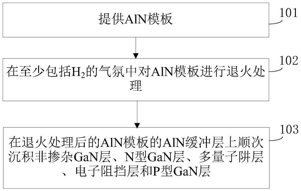
[0039] figure 1 A method of preparation of a GaN-based transmitted emitting diode epitaxial sheet according to an embodiment of the present invention is shown. See figure 1 The method process includes the following steps.

[0040] Step 101 provides an AlN template.

[0041] Among them, the AlN template includes a sapphire substrate and an AlN buffer layer deposited on a sapphire substrate.

[0042] Step 102, at least h 2 The ALN template is annealed in the atmosphere.

[0043] Among them, the annealing treatment time is 5 to 13 min. MIN represents minutes.

[0044] Step 103, sequentially depositing a non-doped GaN layer, an N-type GaN layer, a multi-quantum well layer, an electronic barrier layer, and a P-type GaN layer on the AlN buffer layer of the ALN ...


PUM

PropertyMeasurementUnit
thicknessaaaaaaaaaa
thicknessaaaaaaaaaa
thicknessaaaaaaaaaa

Abstract

The invention discloses a method for preparing GaN-based light-emitting diode epitaxial wafers, belonging to the field of GaN-based light-emitting diodes. The method includes: providing an AlN template, the Al template including a sapphire substrate and an AlN buffer layer deposited on the sapphire substrate; 2 The AlN template is annealed in an atmosphere, and the annealing time is 5 to 13 minutes; a non-doped GaN layer, an N-type GaN layer, and a multi-quantum layer are sequentially deposited on the AlN buffer layer of the AlN template after the annealing treatment. Well layer, electron blocking layer and P-type GaN layer.

Description

Technical field [0001] The present invention relates to the field of GaN-based air optical diodes, and more particularly to a method of preparing a GaN-based transmitted emitting diode epitaxial sheet. Background technique [0002] GaN (gallium nitride) base LED (Light Emitting Diode, LED), also known as GAN-based LED chip, typically comprising an epitaxial piece and an electrode prepared on the epitaxial sheet. The epitaxial sheet generally includes: sapphire substrate, and sequentially laminated ALN buffer layer, non-doped GaN layer, N-type GaN, MQW (Multiple Quantum Well, Multi-quantian well) layer, electron blocking layer, and P-type GaN layer. When there is a current injecting the GaN-based LED, the electron and the hole of the N-type region of the N-type GaN layer and the pockets of the P-type region such as the P-type GaN layer enter the MQW and composite, and the visible light is issued. [0003] The preparation method of existing episodes includes, first, a sapphire subs...

Claims


Application Information

Patent Timeline
Patent Type & Authority Patents(China)
IPC IPC(8): H01L33/00H01L21/02
Inventor 张武斌陶章峰刘旺平周盈盈王坤乔楠吕蒙普胡加辉李鹏
Owner HC SEMITEK ZHEJIANG CO LTD
Learn More