Epitaxial wafer of green light emitting diode and preparation method thereof

A technology of light-emitting diodes and epitaxial wafers, which is applied to semiconductor devices, electrical components, circuits, etc., can solve the problems of uneven distribution of In components, poor uniformity of green light wavelengths, and non-concentrated light-emitting areas, so as to reduce the number of quantum wells. Effects of defects, reduction of uneven distribution of In components, and increase of distribution uniformity

Pending Publication Date: 2022-07-29
JIANGXI ZHAO CHI SEMICON CO LTD
View PDF0 Cites 1 Cited by
  • Summary
  • Abstract
  • Description
  • Claims
  • Application Information

AI Technical Summary

Problems solved by technology

[0003] At present, there are certain defects such as strong polarization electric field and high dislocation density inside the multiple quantum wells, especially for GaN-based LEDs with high In composition such as green LEDs, not only the quantum wells are subject to a larger polarization electric field , and there are more defects, which lead to In clusters inside the multiple quantum wells, the distribution of In components is uneven, and the light-emitting area is not concentrated, resulting in poor wavelength uniformity of green light, which seriously affects the yield

Method used


Image

  • Epitaxial wafer of green light emitting diode and preparation method thereof
  • Epitaxial wafer of green light emitting diode and preparation method thereof
  • Epitaxial wafer of green light emitting diode and preparation method thereof

Examples


Embodiment 1

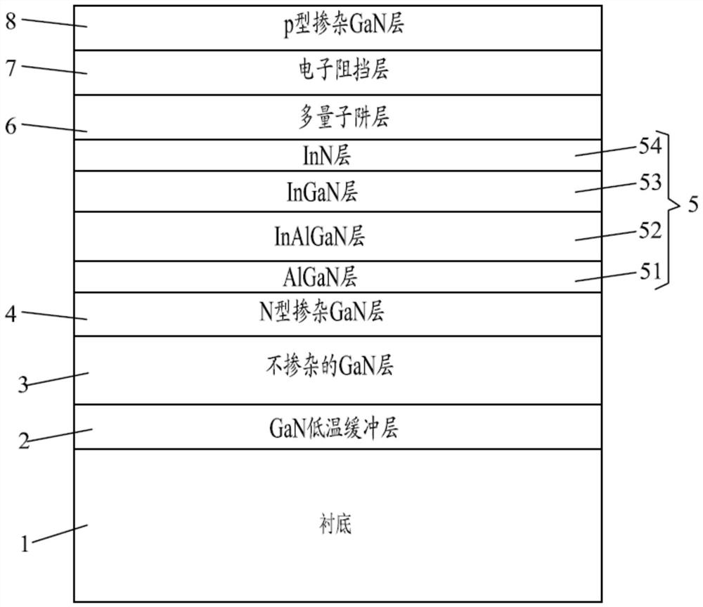
[0037] see figure 1 , shows the epitaxial wafer of the green light emitting diode in the first embodiment of the present invention, including a substrate 1, and a GaN low-temperature buffer layer 2 epitaxially grown on the substrate 1 in turn, an undoped GaN layer 3, N Type doped GaN layer 4 , multiple quantum well preparation layer 5 , multiple quantum well layer 6 , electron blocking layer 7 and p-type doped GaN layer 8 . In this embodiment, a multi-quantum well preparation layer 5 is grown before the multi-quantum well layer 6, that is, a multi-quantum well preparation layer 5 is inserted between the N-type doped GaN layer 4 and the multi-quantum well layer 6, mainly Defects inside the multiple quantum well layer are reduced by the multiple quantum well preparation layer 5, and the uniformity of the emission wavelength is improved.

[0038]Specifically, the multiple quantum well preparation layer 5 includes an AlGaN layer 51 , an InAlGaN layer 52 , an InGaN layer 53 and an...

Embodiment 2

[0068] The second embodiment of the present invention also provides an epitaxial wafer for a green light emitting diode and a preparation method thereof. The epitaxial wafer for a green light emitting diode and its preparation method in this embodiment are the same as the epitaxial wafer for a green light emitting diode in the first embodiment. The difference between and its preparation method is:

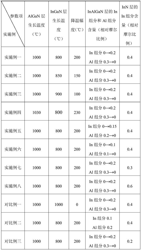
[0069] The growth temperature of the AlGaN layer is 1000°C, the growth temperature of the InGaN layer and the InN layer is 850°C, the growth temperature of the InAlGaN layer is gradually decreased from 1000°C to 850°C, and the growth temperature difference between the AlGaN layer and the InGaN layer is 150°C.

Embodiment 3

[0071] The third embodiment of the present invention also provides an epitaxial wafer for a green light emitting diode and a preparation method thereof. The epitaxial wafer for a green light emitting diode and its preparation method in this embodiment are the same as the epitaxial wafer for a green light emitting diode in the first embodiment. The difference between and its preparation method is:

[0072] The growth temperature of the AlGaN layer is 1000°C, the growth temperature of the InGaN layer and the InN layer is 900°C, the growth temperature of the InAlGaN layer is gradually decreased from 1000°C to 900°C, and the growth temperature difference between the AlGaN layer and the InGaN layer is 100°C.


PUM

PropertyMeasurementUnit
thicknessaaaaaaaaaa
thicknessaaaaaaaaaa
thicknessaaaaaaaaaa

Abstract

The invention provides an epitaxial wafer of a green light emitting diode and a preparation method thereof, the epitaxial wafer of the green light emitting diode comprises a multi-quantum well layer and further comprises a multi-quantum well preparation layer, the multi-quantum well layer grows on the multi-quantum well preparation layer, the multi-quantum well preparation layer comprises an AlGaN layer, an InAlGaN layer, an InGaN layer and an InN layer which sequentially grow in an epitaxial mode, and the AlGaN layer, the InAlGaN layer, the InGaN layer and the InN layer are arranged on the multi-quantum well preparation layer. The multi-quantum well layer is grown on the InN layer. According to the invention, the multi-quantum well preparation layer with a special structural design is grown before the multi-quantum well, so that the defects in the quantum well are successfully reduced, the bottom layer is more matched with the crystal lattice of the quantum well, the stress of the green light multi-quantum well layer is released, an In-rich environment is provided, the incorporation of the green light In component is increased, and the light emitting efficiency is improved. And the polarization effect in the quantum well is reduced, so that the In clustering phenomenon is reduced, the In component distribution is more uniform, the light-emitting area is more uniform, and finally, the light-emitting wavelength uniformity is remarkably improved.

Description

technical field [0001] The invention relates to the technical field of light-emitting diodes, in particular to an epitaxial wafer of a green light-emitting diode and a preparation method thereof. Background technique [0002] As is known to all, light-emitting diodes (Light Emitting Diode, LED for short) have been widely used in solid-state lighting and display fields due to their advantages of high efficiency, energy saving, and environmental protection. Among them, multiple quantum wells are the core structure of LED light-emitting, and the defects of multiple quantum wells will directly affect the quality of LED light-emitting, so multiple quantum wells have always been one of the main research objects in the industry. [0003] At present, there are certain defects such as strong polarization electric field and high dislocation density in the multiple quantum wells. Especially for such high In composition GaN-based LEDs as green LEDs, not only the quantum wells are subjec...

Claims


Application Information

Patent Timeline
Patent Type & Authority Applications(China)
IPC IPC(8): H01L33/06H01L33/32H01L33/12H01L33/00
CPCH01L33/06H01L33/32H01L33/12H01L33/0075
Inventor 张彩霞程金连印从飞胡加辉金从龙
Owner JIANGXI ZHAO CHI SEMICON CO LTD
Why Eureka
Try Eureka