Self-doped silicon-germanium/silicon multiple quantum well thermosensitive material applied to uncooled infrared detection array

An uncooled infrared, detection array technology, applied in electrical radiation detectors, from chemically reactive gases, single crystal growth, etc., can solve problems such as limiting the development of uncooled infrared detection technology, poor MEMS process compatibility, and production line pollution, etc. Achieve the effect of reducing the difficulty of preparation, increasing the allowable range, and improving the absorption performance

Active Publication Date: 2014-03-12
NANJING UNIV OF SCI & TECH
View PDF7 Cites 4 Cited by
  • Summary
  • Abstract
  • Description
  • Claims
  • Application Information

AI Technical Summary

Problems solved by technology

[0003] However, the sensitive material VO x Both α-Si and α-Si have their own shortcomings, which limit the development of uncooled infrared detection technology
Although VO x The temperature coefficient of resistance (TCR) of the thin film is relatively high, but there are problems of poor compatibility with the traditional MEMS process and pollution to the production line; compared with vanadium oxide, the MEMS process compatibility of the α-Si thin film is better, but the TCR is relatively Low, and its amorphous crystal structure makes the 1 / f noise of the material larger

Method used


Image

  • Self-doped silicon-germanium/silicon multiple quantum well thermosensitive material applied to uncooled infrared detection array
  • Self-doped silicon-germanium/silicon multiple quantum well thermosensitive material applied to uncooled infrared detection array
  • Self-doped silicon-germanium/silicon multiple quantum well thermosensitive material applied to uncooled infrared detection array

Examples


Embodiment 1

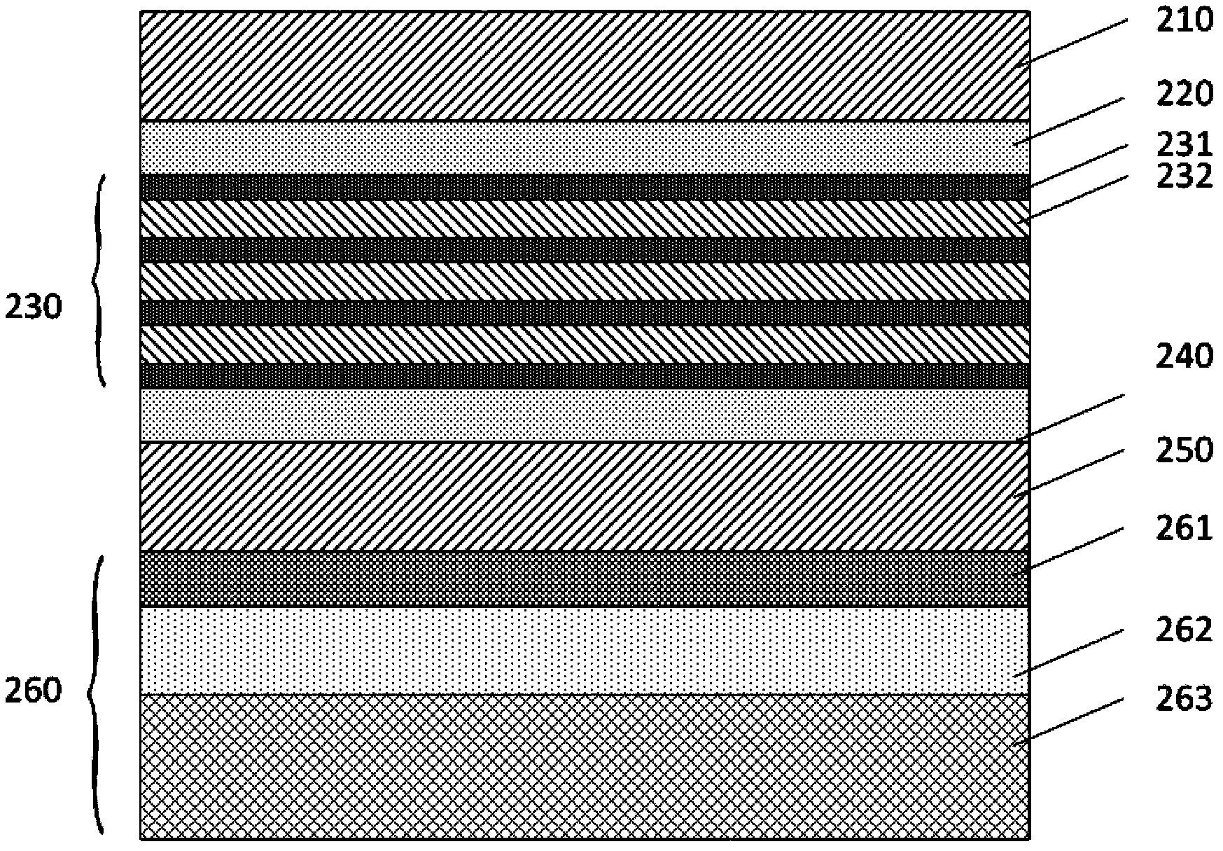
[0053] For the self-doped silicon germanium / silicon multiple quantum well heat-sensitive material used in an uncooled infrared detection array described in the patent of the present invention, when the content of germanium in the silicon germanium layer is 30%, the thickness of the silicon layer 232 (potential barrier) is 30nm, silicon germanium / silicon cycle number is 4 layers; bottom isolation layer 240, top isolation layer 220 is 35nm thick, undoped single crystal silicon; bottom contact layer 250, top contact layer 210 thickness is 150nm, p-type boron doped Heterogeneous single crystal silicon, the doping concentration is 10 19 cm -3 As mentioned above, when the thickness of the single crystal silicon germanium layer 231 in the silicon germanium / silicon multi-quantum well structure 230 is 5nm, 10nm, and 15nm respectively, combined with the position of each energy level and Fermi level in the valence band and the formula (1), the material TCR The corresponding theoretical ...

Embodiment 2

[0055] For the self-doped silicon germanium / silicon multiple quantum well heat-sensitive material used in the uncooled infrared detection array described in the patent of the present invention, when the thickness of the single crystal silicon germanium layer 231 in the silicon germanium / silicon multiple quantum well structure 230 is 10nm , the thickness of the silicon layer 232 (potential barrier) is 30nm, and the silicon germanium / silicon cycle number is 4 layers; the bottom isolation layer 240 and the top isolation layer 220 are 35nm thick, undoped single crystal silicon; the bottom contact layer 250, the top contact Layer 210 has a thickness of 150 nm, p-type boron-doped single crystal silicon, and the doping concentration is 10 19 cm -3 Above, when the contents of germanium in the silicon germanium layer are 25%, 30%, and 35% respectively, combined with the position of each energy level and Fermi energy level in the valence band and the formula (1), the theoretical value o...


PUM

PropertyMeasurementUnit
thicknessaaaaaaaaaa
thicknessaaaaaaaaaa
thicknessaaaaaaaaaa

Abstract

The invention discloses a thermosensitive material which is of a self-doped silicon-germanium/silicon multiple quantum well structure, has a high temperature resistance coefficient and is applied to an uncooled infrared detection array. The material comprises a bottom contact layer, a bottom isolation layer, the silicon-germanium/silicon multiple quantum well structure, a top isolation layer and a top contact layer. When the thickness of each isolation layer is 35 to 100nm, boron particles diffuse from the contact layers to the silicon-germanium/silicon multiple quantum well structure, so as to form a carrier. The design simplifies a process and is conductive to preparing the silicon-germanium/silicon multiple quantum well structure with high lattice quality. The invention discloses a pixel structure of the uncooled infrared detection array which uses the material. The thickness of each support layer in double support layers is 200nm to 250nm. Under the condition that optical conditions are met, the pixel structure is stable. The invention further discloses an extension growth process, which is based on a low pressure chemical vapor deposition technology, of the material.

Description

technical field [0001] The invention belongs to the sensitive material technology for an uncooled infrared detection array, and specifically relates to a heat-sensitive material with a self-doped silicon germanium / silicon multi-quantum well structure and a relatively high temperature resistivity coefficient. Background technique [0002] Infrared imaging technology has a wide range of applications and demands in military and civilian fields. Infrared imaging reflects the information of thermal radiation on the surface of an object and its internal heat dissipation. It is an extension of people's vision beyond the visible light band and a new means of observing and perceiving the objective world. The focal plane array is a sensitive component of infrared imaging, which largely determines the quality of infrared imaging. In the 1970s and 1980s, the cooled infrared focal plane array using mercury cadmium telluride as the sensitive material achieved great success. In the 1990s...

Claims


Application Information

Patent Timeline
Patent Type & Authority Applications(China)
IPC IPC(8): G01J5/20C30B25/16
Inventor 董涛王开鹰姜波何勇杨朝初苏岩
Owner NANJING UNIV OF SCI & TECH
Why Eureka
Try Eureka