Epitaxial structure of gallium nitride device

An epitaxial structure, gallium nitride technology, applied in the field of microelectronics, can solve problems such as poor lattice quality

Pending Publication Date: 2020-04-10
西安电子科技大学芜湖研究院
View PDF3 Cites 3 Cited by
  • Summary
  • Abstract
  • Description
  • Claims
  • Application Information

AI Technical Summary

Problems solved by technology

[0004] The purpose of the present invention is to overcome the problem that the crystal lattice quality of GaN HEMT device is poor at present, provide a kind of HEMT epitaxial structure and preparation method thereof, can improve HEMT Device quality

Method used


Image

  • Epitaxial structure of gallium nitride device
  • Epitaxial structure of gallium nitride device
  • Epitaxial structure of gallium nitride device

Examples


Embodiment 1

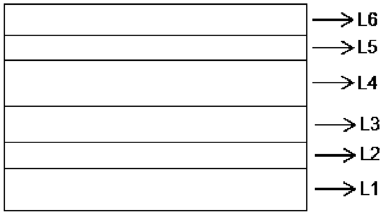
[0018] 1. Provide substrate L1, which is all materials used for epitaxial gallium nitride thin film, including insulating or semi-insulating sapphire, silicon, silicon carbide, gallium nitride and diamond, with a size range of 2-8 inches.

[0019] 2. The nucleation layer L2 is grown at a temperature between 400-700° C., which can be any one or combination of ALN, ALGaN, and GAN, and its total thickness is 10-50 nm.

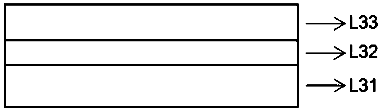
[0020] 3. Growing the buffer layer L3 on the nucleation layer, the growth temperature is between 1050-1130°C. is a cyclic growth pattern composed of three sublayers. It includes the first sub-layer crystal nucleus layer GaN1L31 with a thickness of 20nm, and the total amount of NH3 in the growth environment is 10L / min, which mainly provides crystal nucleus for the subsequent leveling layer. The networked SiNL32 layer is grown on the second sub-layer crystal nucleus layer GaN1L32, its main characteristic is a uniform network structure, which will provide a uniform ...

Embodiment 2

[0025] 1. Provide substrate L1, which is all materials used for epitaxial gallium nitride thin film, including insulating or semi-insulating sapphire, silicon, silicon carbide, gallium nitride and diamond, with a size range of 2-8 inches.

[0026] 2. The nucleation layer L2 is grown at a temperature between 400-700° C., which can be any one or combination of ALN, ALGaN, and GAN, and its total thickness is 10-50 nm.

[0027] 3. Growing the buffer layer L3 on the nucleation layer, the growth temperature is between 1050-1130°C. is a cyclic growth pattern composed of three sublayers. It includes the first sub-layer crystal nucleus layer GaN1L31 with a thickness of 20nm, and the total amount of NH3 in the growth environment is 30L / min, which mainly provides crystal nucleus for the subsequent leveling layer. The networked SiNL32 layer is grown on the second sub-layer crystal nucleus layer GaN1L32, its main characteristic is a uniform network structure, which will provide a uniform ...

Embodiment 3

[0032] 1. Provide substrate L1, which is all materials used for epitaxial gallium nitride thin film, including insulating or semi-insulating sapphire, silicon, silicon carbide, gallium nitride and diamond, with a size range of 2-8 inches.

[0033] 2. The nucleation layer L2 is grown at a temperature between 400-700° C., which can be any one or combination of ALN, ALGaN, and GAN, and its total thickness is 10-50 nm.

[0034] 3. Growing the buffer layer L3 on the nucleation layer, the growth temperature is between 1050-1130°C. is a cyclic growth pattern composed of three sublayers. It includes the first sub-layer crystal nucleus layer GaN1L31 with a thickness of 20nm, and the total amount of NH3 in the growth environment is 50L / min, which mainly provides crystal nucleus for the subsequent leveling layer. The networked SiNL32 layer is grown on the second sub-layer crystal nucleus layer GaN1L32, its main characteristic is a uniform network structure, which will provide a uniform ...


PUM

PropertyMeasurementUnit
thicknessaaaaaaaaaa
thicknessaaaaaaaaaa

Abstract

The invention discloses an epitaxial structure of a gallium nitride device, belongs to the technical field of microelectronics, the epitaxial structure comprises a substrate, a low-temperature nucleating layer, a buffer layer, a high-resistance layer, a channel layer and a barrier layer, wherein the buffer layer is formed by circularly growing GaN<1>/SiN/GaN<2>, comprises a GAN1 crystal nucleus layer, a net-shaped structure SiN thin layer and a GAN2 filling layer, different growth modes are controlled mainly by controlling the total amount of NH3 in the growth environment of the three sub-layers. According to the HEMT device, the dislocation density of the material can be greatly reduced by circularly growing the GaN1/SiN/GaN<2> buffer layer, and the lattice quality is improved, so that the characteristics of electron mobility, breakdown voltage, leakage current and the like of the HEMT device are improved.

Description

technical field [0001] The invention belongs to the field of microelectronic technology, and relates to the epitaxial preparation of semiconductor devices, an epitaxial structure of gallium nitride devices, and the prepared devices are mainly used in high-voltage and high-power applications. Background technique [0002] The third-generation semiconductor material, that is, the Wide Band Gap Semiconductor (WBGS for short) semiconductor material is developed after the first-generation silicon and germanium and the second-generation gallium arsenide and indium phosphide. Among the third-generation semiconductor materials, gallium nitride (GaN) has wide bandgap, direct bandgap, high breakdown electric field, low dielectric constant, high electron saturation drift velocity, strong radiation resistance and good chemical stability Such superior properties as germanium, silicon, and gallium arsenide have become key semiconductor materials for the manufacture of new-generation micro...

Claims


Application Information

Patent Timeline
Patent Type & Authority Applications(China)
IPC IPC(8): H01L29/778H01L29/10H01L21/335
CPCH01L29/7787H01L29/1075H01L29/66462
Inventor 王东吴勇汪琼陈兴严伟伟陆俊葛林男何滇王俊杰曾文秀操焰崔傲袁珂陈军飞张进成
Owner 西安电子科技大学芜湖研究院
Why Eureka
Try Eureka