

P-type cap layer enhanced HEMT device and preparation method thereof
An enhanced, cap layer technology, applied in the field of microelectronics, can solve the problems of affecting the lattice quality of the P-type layer, unable to achieve high hole concentration, increasing electron scattering, etc., to improve the hole carrier concentration and mobility, Epitaxial preparation ensures and reduces the effect of electron scattering
- Summary
- Abstract
- Description
- Claims
- Application Information
AI Technical Summary
Problems solved by technology
Method used
Image

Examples
Embodiment 1
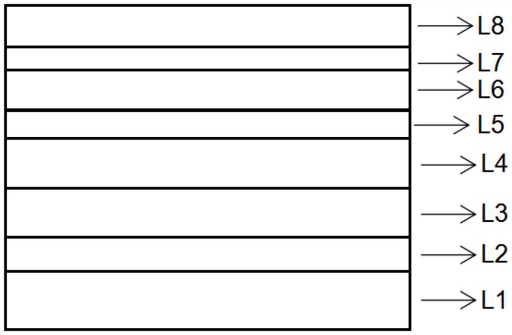
[0035] (1) Substrate L1 is provided, which is all materials used for epitaxial gallium nitride thin film, including insulating or semi-insulating sapphire, silicon, silicon carbide, gallium nitride and diamond, with a size range of 2 inches.
[0036] (2) The nucleation layer L2 is grown at a temperature of 400° C., which can be any one or a combination of ALN, ALGaN, and GAN, and its total thickness is 10 nm.
[0037] (3) A buffer layer L3 is grown on the nucleation layer, which is made of AlGaN material, the growth temperature is 900°C, and the film thickness is 0.5um.
[0038] (4) Continue to grow the non-intentionally doped GaN high-resistance layer L4 on the buffer layer, the thickness of the film is 1.5um, and the growth temperature is between 1120°C.
[0039] (5) A gallium nitride channel layer L5 is grown on the high-resistance layer, and the film thickness range is 50nm.
[0040] (6) The structural formula of the barrier layer L6 on the channel layer is ALGaN, the thi...
Embodiment 2
[0044] (1) Substrate L1 is provided, which is all materials used for epitaxial gallium nitride thin films, including insulating or semi-insulating sapphire, silicon, silicon carbide, gallium nitride and diamond, with a size range of 5 inches.
[0045] (2) The nucleation layer L2 is grown at a temperature of 500° C., which can be grown by any one or a combination of ALN, ALGaN, and GAN, and its total thickness is 40 nm.
[0046](3) A buffer layer L3 is grown on the nucleation layer, which is made of AlGaN material, the growth temperature is 1000° C., and the film thickness is 1 μm.
[0047] (4) Continue to grow the unintentionally doped gallium nitride high-resistance layer L4 on the buffer layer, the film thickness range is 2um, and the growth temperature is between 1135°C.
[0048] (5) A gallium nitride channel layer L5 is grown on the high resistance layer, and the film thickness range is 100nm.
[0049] (6) The structural formula of the barrier layer L6 on the channel laye...
Embodiment 3
[0053] (1) Substrate L1 is provided, which is all materials used for epitaxial gallium nitride thin film, including insulating or semi-insulating sapphire, silicon, silicon carbide, gallium nitride and diamond, with a size range of 8 inches.
[0054] (2) The nucleation layer L2 is grown at a temperature of 700° C., which can be grown by any one or a combination of ALN, ALGaN, and GAN, and its total thickness is 50 nm.
[0055] (3) A buffer layer L3 is grown on the nucleation layer, which is made of AlGaN material, the growth temperature is 1120°C, and the film thickness is 2um.
[0056] (4) Continue to grow the unintentionally doped GaN high-resistance layer L4 on the buffer layer, the film thickness range is 3um, and the growth temperature is between 1150°C.
[0057] (5) A gallium nitride channel layer L5 is grown on the high resistance layer, and the film thickness range is 200nm.
[0058] (6) The structural formula of the barrier layer L6 on the channel layer is ALGaN, the...
PUM
| Property | Measurement | Unit |
|---|---|---|
| thickness | aaaaa | aaaaa |
| thickness | aaaaa | aaaaa |
| thickness | aaaaa | aaaaa |
Abstract
Description
Claims
Application Information