Light-emitting diode epitaxial wafer and preparation method thereof

A technology of light-emitting diodes and epitaxial wafers, applied in electrical components, circuits, semiconductor devices, etc., can solve the problem of P-type semiconductor layer affecting the expansion of holes, and achieve forward voltage reduction, antistatic ability improvement, and antistatic ability. strong effect

Active Publication Date: 2019-02-15
HC SEMITEK ZHEJIANG CO LTD
View PDF4 Cites 0 Cited by
  • Summary
  • Abstract
  • Description
  • Claims
  • Application Information

AI Technical Summary

Problems solved by technology

[0006] The embodiment of the present invention provides a light-emitting diode epitaxial wafer and its preparation method, which can solve the problem that many defects in the P-type semiconductor layer in the prior art will affect the expansion of holes

Method used


Image

  • Light-emitting diode epitaxial wafer and preparation method thereof
  • Light-emitting diode epitaxial wafer and preparation method thereof
  • Light-emitting diode epitaxial wafer and preparation method thereof

Examples


Embodiment Construction

[0029] In order to make the object, technical solution and advantages of the present invention clearer, the implementation manner of the present invention will be further described in detail below in conjunction with the accompanying drawings.

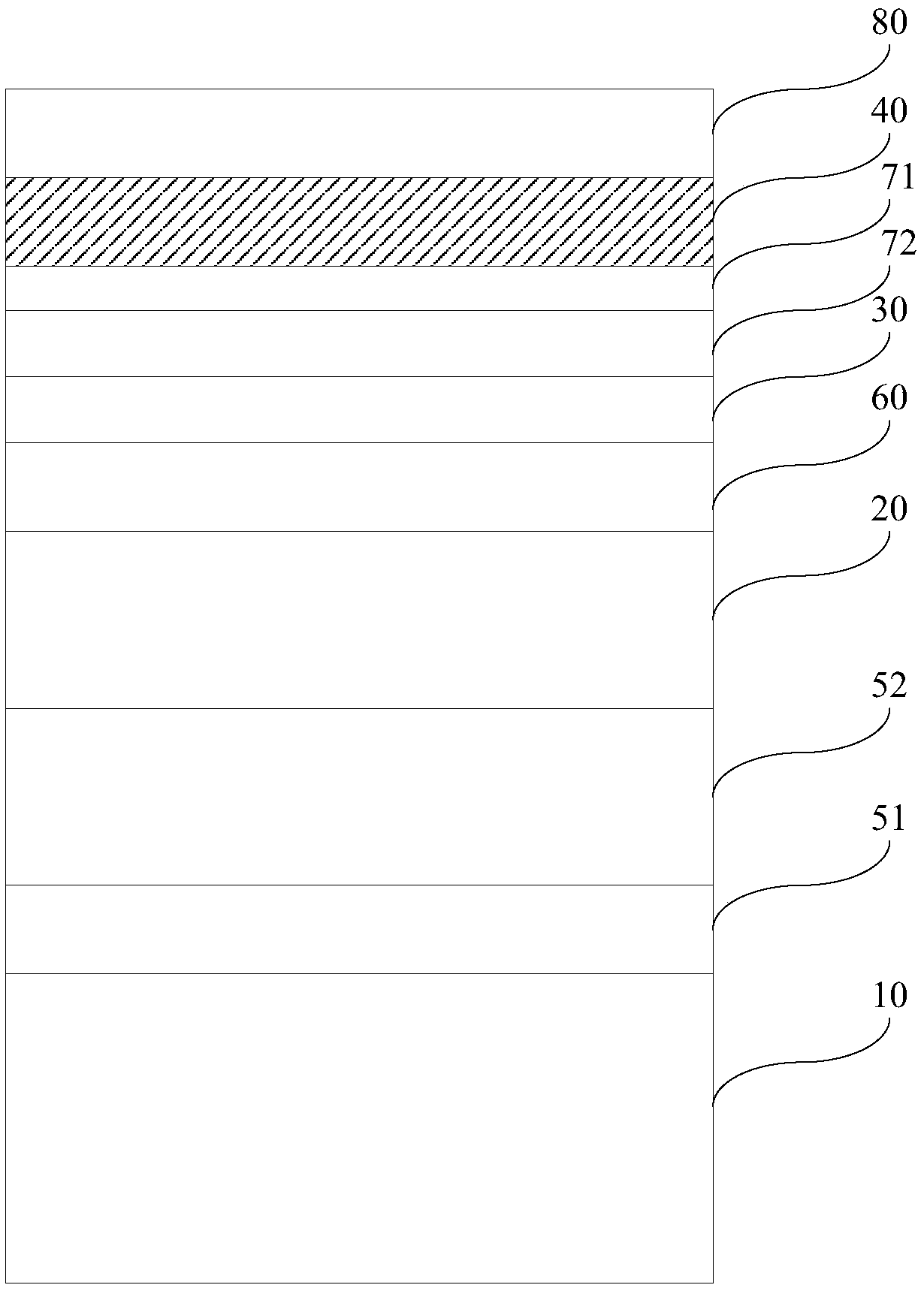
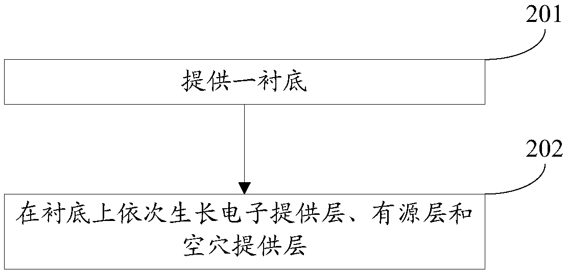
[0030] An embodiment of the present invention provides a light emitting diode epitaxial wafer. figure 1 A schematic structural diagram of a light emitting diode epitaxial wafer provided by an embodiment of the present invention. see figure 1 The light emitting diode epitaxial wafer includes a substrate 10 , an electron supply layer 20 , an active layer 30 and a hole supply layer 40 , and the electron supply layer 20 , the active layer 30 and the hole supply layer 40 are stacked on the substrate 10 in sequence.

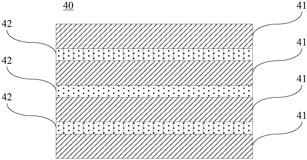
[0031] figure 2 Schematic diagram of the structure of the hole-providing layer provided for the embodiment of the present invention. see figure 2 , in this embodiment, the hole providing layer 40 includes a first sublayer...


PUM

PropertyMeasurementUnit
Thicknessaaaaaaaaaa

Abstract

The invention discloses a light-emitting diode epitaxial wafer and a preparation method thereof, and belongs to the technical field of semiconductors. The light-emitting diode epitaxial wafer comprises a substrate, an electron providing layer, an active layer and a hole providing layer, wherein the electron providing layer, the active layer and the hole providing layer are laminated on the substrate in sequence; the hole providing layer comprises a first sub layer and at least one second sub layer inserted into the first sub layer; the first sub layer is made from magnesium-doped gallium nitride; the second sub layer is made from carbon-doped gallium nitride; and the thickness of the first sub layer is greater than 1 / 2 of the thickness of the hole providing layer. The at least one carbon-doped gallium nitride layer is inserted into the magnesium-doped gallium nitride layer, so that plane spreading of holes is realized, the series resistance of the hole providing layer is reduced, and the anti-static capacity of an LED is strengthened.

Description

technical field [0001] The invention relates to the technical field of semiconductors, in particular to a light-emitting diode epitaxial wafer and a preparation method thereof. Background technique [0002] A light-emitting diode (English: Light Emitting Diode, referred to as: LED) is a semiconductor electronic component that can emit light. Gallium nitride (GaN) has good thermal conductivity, and has excellent characteristics such as high temperature resistance, acid and alkali resistance, and high hardness, so that gallium nitride (GaN)-based LEDs have received more and more attention and research. [0003] Epitaxial wafers are the primary products in the LED manufacturing process. The existing LED epitaxial wafer includes a substrate, an N-type semiconductor layer, an active layer and a P-type semiconductor layer, and the N-type semiconductor layer, the active layer and the P-type semiconductor layer are sequentially stacked on the substrate. The P-type semiconductor la...

Claims


Application Information

Patent Timeline
IPC IPC(8): H01L33/32H01L33/24H01L33/00
CPCH01L33/0066H01L33/0075H01L33/24H01L33/325
Inventor 郭炳磊王群葛永晖吕蒙普李鹏
Owner HC SEMITEK ZHEJIANG CO LTD
Why Eureka
Try Eureka