

Avalanche tolerance test device of power MOSFET device
A technology of avalanche tolerance and testing equipment, which is applied in the direction of single semiconductor device testing, etc., can solve the problems of bulky measuring equipment and high cost, and achieve the effects of cost reduction, low equipment cost and simple testing scheme
- Summary
- Abstract
- Description
- Claims
- Application Information
AI Technical Summary
Problems solved by technology
Method used
Image

Examples
Embodiment Construction
[0026] In order to describe the present invention more specifically, the technical solutions of the present invention will be described in detail below in conjunction with the accompanying drawings and specific embodiments.
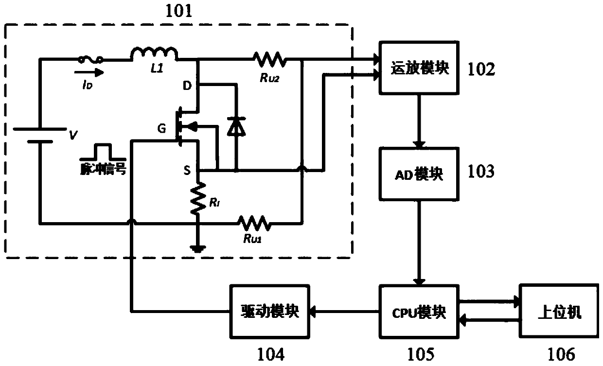
[0027] Such as figure 1 As shown, the test device for avalanche tolerance of power MOSFET devices in the present invention includes a front-end avalanche test circuit, a back-end avalanche voltage and current sampling circuit and a control module.
[0028]The structure of the front-end avalanche test circuit 101 includes an adjustable DC power supply V, a fuse, an adjustable inductance L1, a power MOSFET device to be tested and a current sampling resistor R I ; The positive pole of the adjustable DC power supply V is connected to the fuse; the other end of the fuse is connected to the inductor L1; the other end of the inductor L1 is connected to the drain of the MOSFET device to be tested; the source of the MOSFET device to be tested is connected to the c...
PUM
 Abstract
Description
Claims
Application Information