Broad-spectrum multi-band detection structure with enhanced selective absorption and its preparation method
A wide-spectrum, selective technology for photodetection
- Summary
- Abstract
- Description
- Claims
- Application Information
AI Technical Summary
Problems solved by technology
Method used
Image
Examples
Embodiment Construction
[0024] The present invention will be described in detail below in conjunction with the accompanying drawings and specific embodiments.
[0025] The basic principles and ideas of this application are:
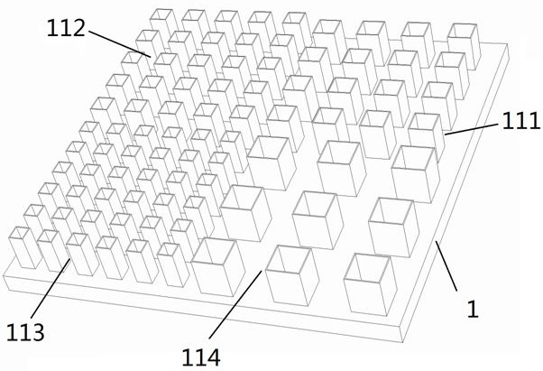
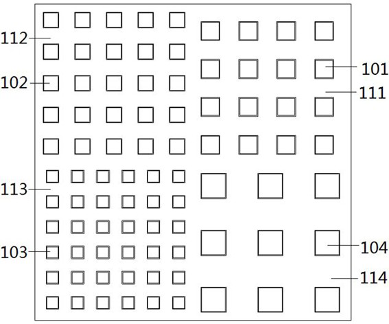
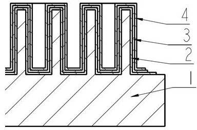
[0026] The base of the wide-spectrum detection structure is an array of three-dimensional square well microstructures, and there are resonant cavities in the square well microstructures and between the square well microstructures. A microlens array is arranged above the subpixel unit composed of the square well microstructure array and the lower electrode 2 on its surface, the photosensitive layer 3 and the upper electrode 4, and each microlens is opposite to the subpixel unit below, and the microlens will incident The light waves converge, pass through the filter, and enter the wide-spectrum detection structure. Most of the light waves hit the resonant cavity, and a small part hit the non-resonant place. The incident light wave passes through the upper electrode 4 which is con...
PUM
| Property | Measurement | Unit |
|---|---|---|
| thickness | aaaaa | aaaaa |
| height | aaaaa | aaaaa |
Abstract
Description
Claims
Application Information


